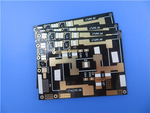
This PCB utilizes F4BTM300 as its base material, features an Electroless Nickel Immersion Gold (ENIG) surface finish, and strictly conforms to IPC-Class-2 quality standards. It adopts a 2-layer rigid structure, tailored to meet the high-performance demands of aerospace, military, and phase-sensitive electronic systems.
PCB Specifications
| Construction Parameter |
Specification |
| Base Material |
F4BTM300 (composite of glass fiber cloth, nano-ceramic fillers, and PTFE resin) |
| Layer Count |
2-layer rigid structure |
| Board Dimensions |
112mm × 89mm per unit, with a dimensional tolerance of ±0.15mm |
| Minimum Trace/Space |
Minimum 4 mils / 5 mils |
| Minimum Hole Size |
0.4mm |
| Blind Vias |
Not incorporated |
| Finished Board Thickness |
0.3mm |
| Finished Copper Weight |
1oz (1.4 mils) on both outer layers |
| Via Plating Thickness |
20 μm, ensuring dependable interlayer conductivity |
| Surface Finish |
Electroless Nickel Immersion Gold (ENIG) |
| Silkscreen |
No silkscreen applied to either top or bottom layer |
| Solder Mask |
Black solder mask on the top layer; no solder mask on the bottom layer |
| Quality Control |
100% electrical test before shipment |
Stack-up Configuration
| Layer Name |
Material |
Thickness |
| Top Copper Layer (Copper_layer_1) |
Copper |
35 μm |
| Substrate Core |
F4BTM300 |
0.254mm (10 mil) |
| Bottom Copper Layer (Copper_layer_2) |
Copper |
35 μm |

F4BTM300 Material Introduction
F4BTM series laminates are produced through a precision manufacturing process, blending glass fiber cloth, nano-ceramic fillers, and polytetrafluoroethylene (PTFE) resin in a scientifically formulated mixture. Built on the F4BM dielectric layer, F4BTM300 incorporates high-Dk, low-loss nano-ceramics, yielding enhanced dielectric constant, superior heat resistance, reduced thermal expansion coefficient, elevated insulation resistance, and improved thermal conductivity—all while maintaining low-loss performance.
F4BTM300 laminates are specifically matched with reverse-treated RTF copper foil, delivering excellent PIM performance, precise line accuracy, and minimized conductor loss. These characteristics make it ideal for demanding applications that require stable performance across extreme temperature ranges and harsh operating environments.
F4BTM300 Material Features
| Category |
Feature |
Specification |
| Electrical Properties |
Dielectric Constant (Dk) |
3.0 ± 0.06 at 10GHz |
| Dissipation Factor |
0.0018 at 10GHz; 0.0023 at 20GHz |
| Thermal Stability |
CTE (XYZ Axes) |
15/16/72 ppm/°C (-55°C to 288°C) |
| Thermal Coefficient of Dk |
-75 ppm/°C (-55°C to 150°C) |
| Physical Properties |
Moisture Absorption |
0.05% |
| Flammability Rating |
UL 94-V0 |
F4BTM300 Material Benefits
-Superior Electrical Performance: Paired with reverse-treated RTF copper foil to deliver excellent PIM performance, precise line control, and minimized conductor loss.
-Enhanced Environmental Adaptability: Combines low moisture absorption, high heat resistance, and stable performance from -55°C to 288°C, suitable for harsh environments.
-Balanced Dielectric & Thermal Traits: Integrates high Dk, low loss, and improved thermal conductivity to support high-power and high-frequency operations.
-Robust Insulation: Offers increased insulation resistance, ensuring reliable isolation in precision electronic assemblies.
Typical Applications
Aerospace & Cabin Equipment
Microwave/RF Systems
Radar & Military Radar Equipment
Feed Networks
Phase-Sensitive & Phased Array Antennas
Satellite Communication Systems
Quality & Availability
This PCB meets IPC-Class-2 quality standards, ensuring reliable performance for commercial, military, and aerospace electronic systems. Artwork is provided in the industry-standard Gerber RS-274-X format, compatible with global manufacturing processes. It is available worldwide, supporting global projects and timely international delivery.

 Your message must be between 20-3,000 characters!
 English