Bicheng Electronics Technology Co., Ltd
We Are Your RF PCB Solution Provider!
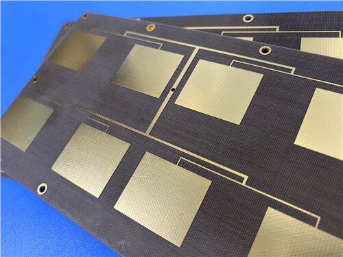
Rogers PCB, Taconic PCB, Arlon PCB, F4B PCB
ISO9001, ISO14001, IATF 16949 certified
Detail Information
Main Market:
North America
, South America
, Western Europe
, Eastern Europe
, Southeast Asia
, Africa
, Oceania
, Worldwide
Business Type:
Manufacturer
, Distributor/Wholesaler
, Exporter
, Seller
No. of Employees:
350~450
Annual Sales:
10 million-18 million
Detail Description
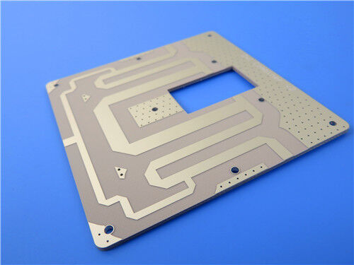
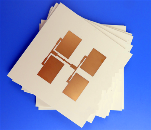
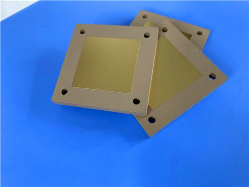
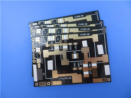
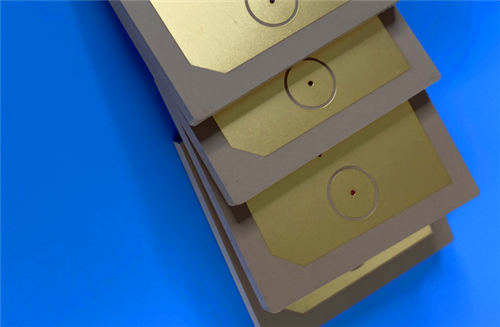
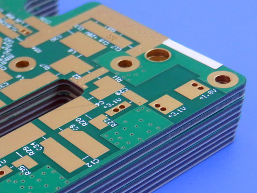
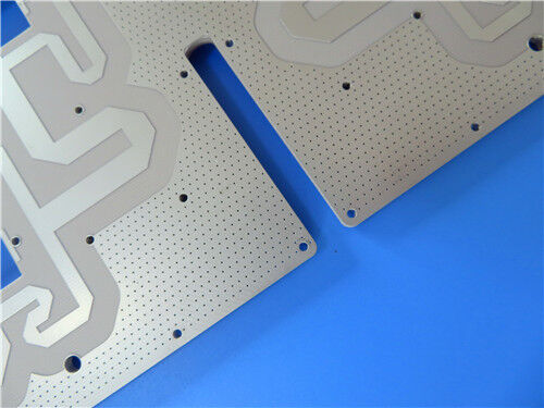
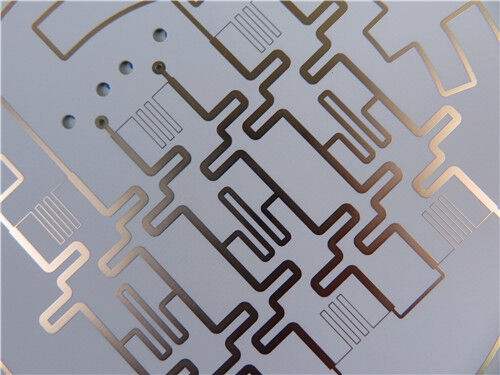
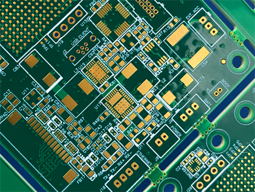
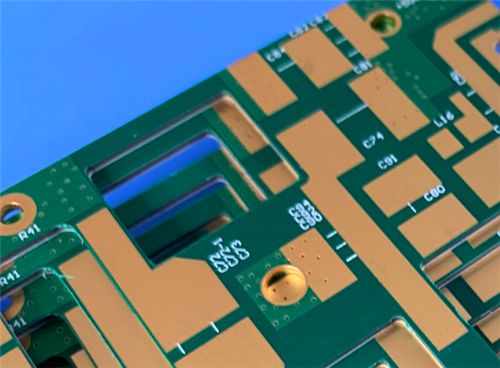
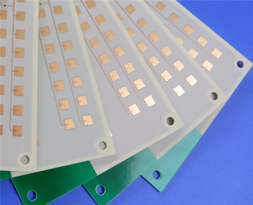
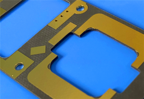
Founded in 2003, Shenzhen Bicheng Electronics Technology Co., Ltd. is a well-established supplier and exporter of high-frequency PCBs based in Shenzhen, China. With 23 years of industry experience, the company serves global sectors such as cellular base station antennas, satellite communications, high-frequency passive components, microstrip and stripline circuits, millimeter-wave equipment, radar systems, and digital RF antennas. Bicheng's high-frequency PCBs are primarily manufactured using three major high-frequency material brands—Rogers Corporation, Taconic, and Wangling—with dielectric constants ranging from 2.2 to 10.2. Headquartered in the economically vibrant city of Shenzhen, Bicheng PCB operates with a philosophy centered on serving small and medium-sized enterprises, offering a wide variety of circuit boards to meet diverse market demands.
Main Business & PCB Applications
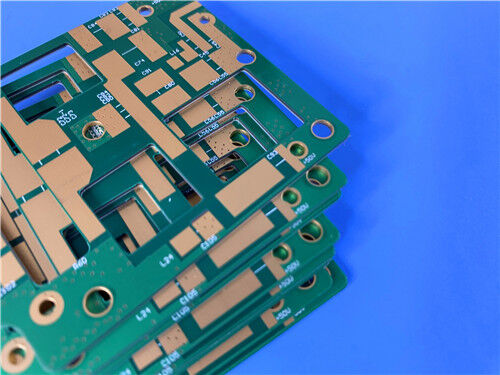
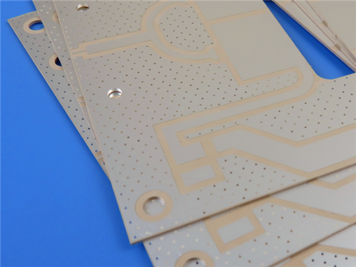
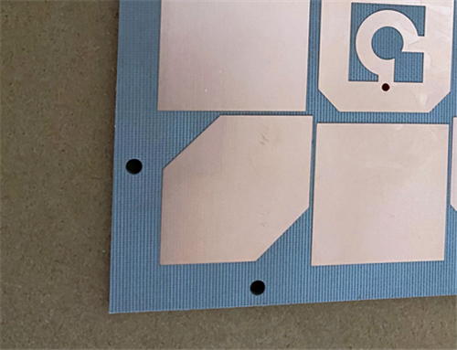
The company upholds the highest manufacturing standards to deliver products known for exceptional quality, performance, and reliability. In addition to high-frequency PCBs, Bicheng has divisions specializing in FR-4 circuit boards, high frequency PCBs, and RF PCBs, supporting everything from prototyping and small-batch production to mass manufacturing. The company actively develops value-added PCB solutions, including HDI, quick-turn production, impedance control, heavy copper, and backplane boards. This strategic focus enables Bicheng to offer an extended and complementary product range, forming an integrated line that spans from low-end to high-end PCBs. These circuit boards are widely used in home appliances, portable and consumer electronics, medical devices, aerospace, and telecommunications.
Main Material Partners

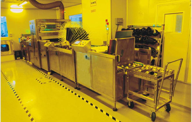
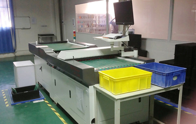
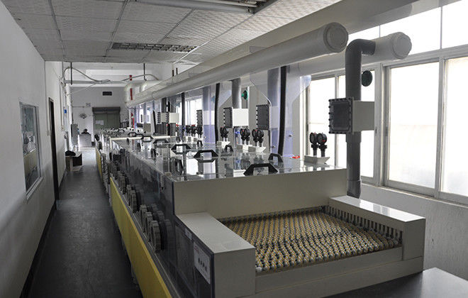
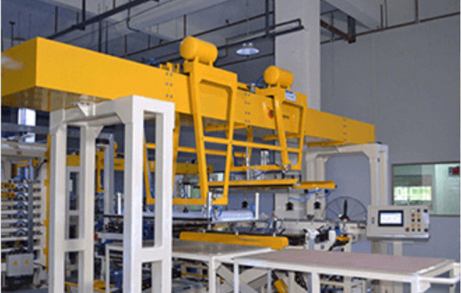
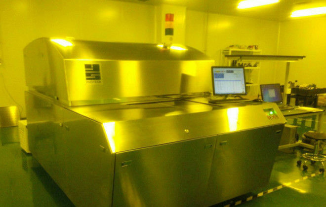
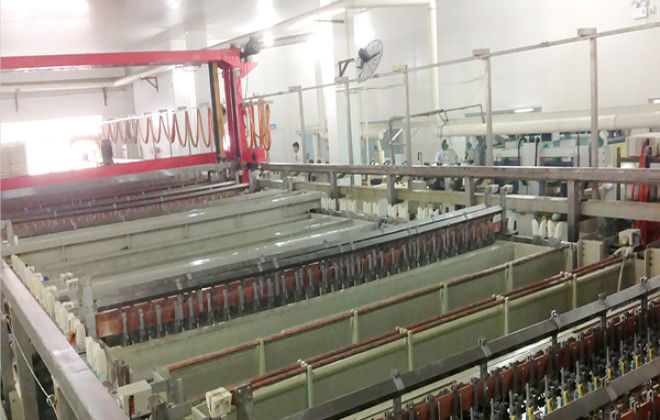
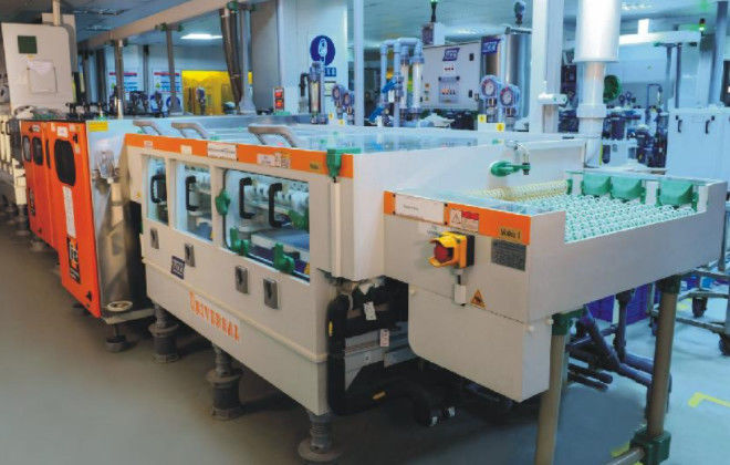
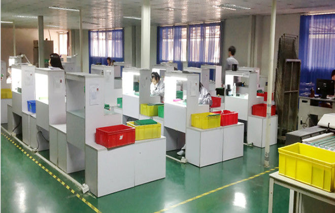
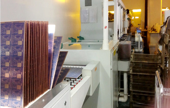
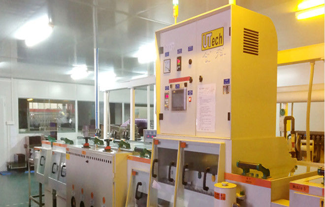
production line
Bicheng Electronics operates two major production bases, strategically located in Shenzhen and Jiangmen.
The Shenzhen factory employs over 300 staff and has a monthly output exceeding 10,000 square meters of PCBs. As a brand-new facility, it specializes in quick-turn prototypes and small-volume production.
The Jiangmen factory features two new industrial buildings spanning approximately 15,000 square meters, specifically designed for mass production. Equipped with state-of-the-art automated machinery sourced from Israel, Japan, Germany, and Taiwan, the Jiangmen facility produces up to 30,000 square meters per month for 2- to 10-layer PCBs. The establishment of this plant has significantly strengthened Bicheng’s capacity to supply high-end PCBs to both domestic and global markets.
With a strong and diverse product portfolio, Bicheng serves customers worldwide. Our offerings include multi-layer boards (up to 32 layers), flex-rigid combinations, heavy copper PCBs, high-frequency and high-speed boards, and HDI, among other types.
We are committed to becoming a leading diversified PCB supplier known for precision-engineered products. Our mission is to create lasting value for our customers while building a promising future for our employees.
oem/odm
One-Stop PCB OEM/ODM – Our Network Is Your Strength
Stop managing multiple PCB suppliers. We connect you with China's the most capable PCB manufacturers. You share your requirements – we handle the rest.
Service Scope:
Quick-turn / Prototypes – 1–8 layers, 24/48/72h rush available.
Volume production – 4–20 layers, cost-optimized, 7–15 days lead time.
Specialty boards – High-frequency (Rogers/PTFE), Aluminum-core, Heavy copper (3–10 oz).
Our OEM/ODM Workflow:
Requirement analysis – You send Gerbers or sketches → We assess difficulty and cost.
Best-factory matching – Select 2–3 suitable factories from our partner pool (e.g., Fab A for high-layer, Fab B for quick-turn).
On-site quality supervision – Our QC follows key processes (lamination, drilling, plating).
Unified delivery – Multi-factory orders consolidated, relabeled, and shipped to your door.
Client Benefits:
15–25% cost reduction – Through comparison sourcing and consolidated purchasing.
Controllable lead times – Orders diversion when one fab is overloaded.
One-stop purchasing – No need to manage 5 PCB fabs.
PCB Pattern Plating
PCB Washing
Developing
R&D
Design For Manufacture
| Serial NO. |
Procedure |
Item |
Manufacturing capability |
| Large volume (S<100 m²) |
Middle volume (S<10 m²) |
Prototype(S<1m²) |
| 1 |
Inner layer (18um, 35um, 70um etc are finished copper. If not mentioned copper, finished 1oz is the default value ) |
Min.isolation of layers |
0.1mm |
0.1mm |
0.06mm |
| 2 |
Min.track and spacing |
5/5mil(18um) |
4/4mil(18um) |
3/3.5mil(18um) |
| 3 |
5/5mil(35um) |
4/4mil(35um) |
3/4mil(35um) |
| 4 |
7/9mil(70um) |
6/8mil(70um) |
6/7mil(70um) |
| 5 |
9/11mil(105um) |
8/10mil(105um) |
8/9mil(105um) |
| 6 |
13/13mil(140um) |
12/12mil(140um) |
12/11mil(140um) |
| 7 |
Min.distance from drill to conductor |
4 Layer 10mil,6 layer 10mil,8-12 layer 12mil |
4 layer 8mil,6 layer 8mil,8-12 layer 10mil,14-20 layer 14mil,22-32 layer 18mil |
4 layer 6mil,6 layer 6mil,8-14 layer 8mil,16-22 layer 12mil,24-32 layer 14mil |
| 8 |
Min.width of annular ring on inner layer |
4 Layer 10mil(35um),≥6 Layer 14mil(35um) |
4 Layer 8mil(35um),≥6 layer 12mil(35um) |
4 Layer 6mil(35um),≥6 Layer 10mil(35um) |
| 9 |
Inner layer isolation ring width(Min) |
10mil (35um) |
8mil (35um) |
6mil (35um) |
| 10 |
Min.via pad diameter |
20mil (35um) |
16mil (35um) |
16mil (35um) |
| 11 |
Min. distance from board edge to conductor(no copper exposured)(inner layer) |
14 mil(35um) |
12 mil(35um)) |
8 mil(35um) |
| 12 |
Maximum copper weight(Inner layer and outer layer) |
3 OZ( 105 um ) |
4 OZ ( 140 um ) |
6 OZ( 210 um ) |
| 13 |
Core with different copper foil on both sides |
/ |
18/35,35/70 um |
18/35,35/70 um |
| 14 |
Laminating |
Tolerance of laminate thickness |
±10% PCB thick |
±10% PCB thick |
±8% PCB thick |
| 15 |
Maximum laminate thickness |
4.0mm |
6.0mm |
7.0mm |
| 16 |
Laminate alignment accuracy |
≤±5 mil |
≤±4 mil |
≤±4 mil |
| 17 |
Drill (18um, 35um, 70um etc are finished copper. If not mentioned copper, finished 1oz is the default value ) |
Min.drill bit diameter |
0.2 mm |
0.2 mm |
0.2 mm |
| 18 |
Min.slot router diameter |
0.60 mm |
0.60 mm |
0.60 mm |
| 19 |
Min.tolerance of PTH slots |
±0.15mm |
±0.15mm |
±0.1mm |
| 20 |
Max.aspect ratio |
1:08 |
1:12 |
1:12 |
| 21 |
Hole tolerance |
±3mil |
±3mil |
±3mil |
| 22 |
Space of via to via |
6mil(same net),12mil(different net) |
6mil(same net),14mil(different net) |
4mil(same net),12mil(different net) |
| 23 |
Space of component hole to component hole |
12mil(same net),16mil(different net) |
12mil(same net),16mil(different net) |
10mil(same net),14mil(different net) |
| 24 |
Etching |
Min.width of etching logo |
10mil(18um),12 mil (35um),12 mil(70um) |
8mil(18um),10mil(35um),12 mil(70um) |
6mil(18um),8 mil(35um),12mil(70um) |
| 25 |
Etch factor |
1.6-2.2 |
1.6-2.2 |
1.6-2.2 |
| 26 |
Outer layer(18um, 35um, 70um etc are finished copper. If not mentioned copper, finished 1oz is the default value ) |
Min.via pad diameter |
20mil |
16mil |
16mil |
| 27 |
Min.BGA pad diameter |
12mil |
12mil |
10mil |
| 28 |
Min.track and spacing |
5/5mil(18um) |
4/4mil(18um) |
3/3.5mil(18um) |
| 5/5mil(35um) |
4/4mil(35um) |
3/4mil(35um) |
| 7/9mil(70um) |
6/8mil(70um) |
6/7mil(70um) |
| 9/11mil(105um) |
8/10mil(105um) |
8/9mil(105um) |
| 13/13mil(140um) |
12/12mil(140um) |
12/11mil(140um) |
| 29 |
Minimum grid |
10/10mil(35um) |
8/8mil(35um) |
4/8mil(35um) |
| 30 |
Min.space (conductor to pad, pad to pad) |
6mil(18um) |
5mil(18um) |
4mil(18um) |
| 6mil(35um) |
5mil(35um) |
4mil(35um) |
| 9mil(70um) |
8mil(70um) |
7mil(70um) |
| 11mil(105um) |
10mil(105um) |
9mil(105um) |
| 13mil(140um) |
12mil(140um) |
11mil(140um) |
| 31 |
Solder mask (18um, 35um, 70um etc are finished copper. If not mentioned copper, finished 1oz is the default value ) |
Maximum via-plug diameter |
0.5mm |
0.5mm |
0.5mm |
| 32 |
Min.width of solder mask bridge |
Green:5mil(35um) |
Green:4mil(35um) |
Green:4mil(35um) |
| 33 |
Yellow:5mil(35um) |
Yellow:4mil(35um) |
Yellow:4mil(35um) |
| 34 |
Blue:5mil(35um) |
Blue:4mil(35um) |
Blue:4mil(35um) |
| 35 |
Black:6mil(35um) |
Black:6mil(35um) |
Black:6mil(35um) |
| 36 |
White:6mil(35um) |
White:6mil(35um) |
White:6mil(35um) |
| 37 |
All of Matt:6mil |
All of Matt:6mil |
All of Matt:6mil |
| 38 |
Green:5mil(70um) |
Green:4mil(70um) |
Green:4mil(70um) |
| 39 |
Yellow:5mil(70um) |
Yellow:4mil(70um) |
Yellow:4mil(70um) |
| 40 |
Blue:5mil(70um) |
Blue:4mil(70um) |
Blue:4mil(70um) |
| 41 |
Black:6mil(70um) |
Black:6mil(70um) |
Black:6mil(70um) |
| 42 |
White:6mil(70um) |
White:6mil(70um) |
White:6mil(70um) |
| 43 |
Open solder mask |
4mil(35um) |
4mil(35um) |
3mil(35um) |
| 44 |
Solder mask coverage |
4mil(35um) |
4mil(35um) |
3mil(35um) |
| 45 |
Min.width of solder mask text |
9mil(35um) |
9mil(35um) |
8mil(35um) |
| 46 |
Min.thickness of Solder mask |
9um(35um) |
9um(35um) |
9um(35um) |
| 47 |
Max.thickness of solder mask |
30um(35um) |
30um(35um) |
30um(35um) |
| 48 |
Silkscreen |
Min.width of silkscreen text |
6mil |
6mil |
5mil |
| 49 |
Min.height of silkscreen text |
35mil |
35mil |
30mil |
| 50 |
Min.space from silkscreen to pads |
6mil |
6mil |
5mil |
| 51 |
Colour of silkscreen |
White, Black, Yellow |
| 52 |
Carbon ink |
Carbon ink covers conductor or pads |
14mil |
13mil |
12mil |
| 53 |
Mid distance from carbon ink to pads |
12mil |
11mil |