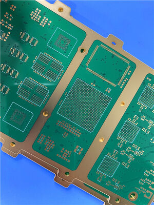
This 14-layer high-speed low-loss PCB is fabricated using M6 high-performance substrate, which is specifically engineered for high-speed signal transmission applications. It strictly adheres to IPC-3 quality standards, featuring a finished board thickness of 2.406mm, and incorporates professional manufacturing processes including 5-point impedance control, 0.2mm via holes with resin plugging, and electroplating leveling. The product exhibits superior signal integrity and structural stability, making it suitable for high-speed, high-precision electronic equipment that demands low signal loss and stringent impedance control.
PCB Specifications
| Specification Item |
Technical Specification |
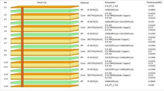
| Layer Configuration |
14-Layer Rigid PCB |
| Base Substrate Material |
M6 High-Speed Low-Loss Multi-layer Material |
| Finished Board Thickness |
2.406 mm |
| Board Dimensions |
106mm × 102mm (per unit), 1 piece per unit |
| Copper Weight (Inner Layers) |
0.5 oz (Finished Copper) |
| Copper Weight (Outer Layers) |
1 oz (Finished Copper) |
| Surface Finish |
Nickel-Palladium-Gold (NiPdAu) |
| Solder Mask & Silkscreen |
Green Solder Mask with White Silkscreen Text |
| Quality Standard |
IPC-3 Standard Compliant |
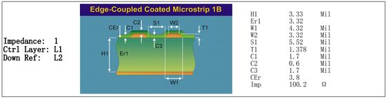
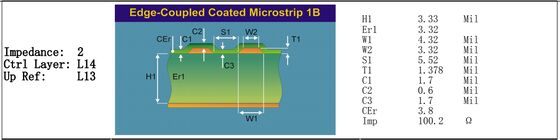
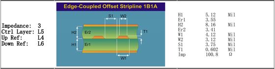
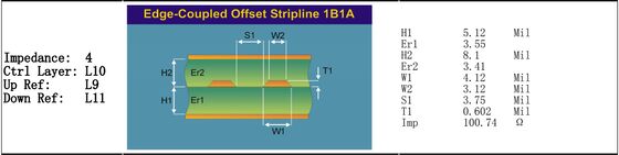
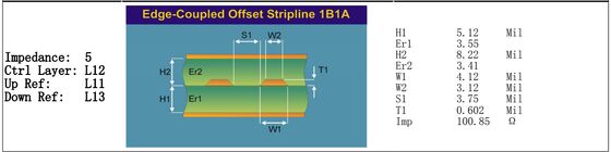
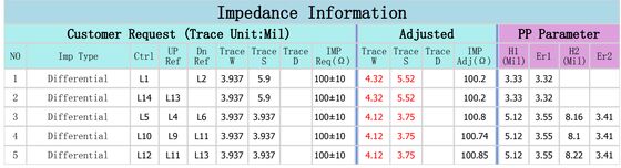
| Impedance Control |
5 Points of Impedance Control (Precision Controlled) |
| Via Hole Specifications & Processes |
1. Via Hole Diameter: 0.2 mm; 2. Special Processes: Resin Plugging + Electroplating Leveling |

M6 High-Speed Low-Loss Multi-layer Material Introduction
M6 is a high-performance high-speed low-loss multi-layer substrate, typically produced by Isola Company as a ceramic-filled epoxy resin system (improved FR-4 type). It is specially developed for high-speed, high-frequency circuit applications, integrating excellent electrical performance, mechanical stability and processing compatibility. Compared with traditional FR-4 substrates, M6 has lower signal loss and more stable dielectric properties, which can effectively ensure the integrity of high-speed signals (10Gbps+) and meet the strict requirements of multi-layer PCB for material performance. At the same time, it balances performance and cost, with performance close to PTFE materials but lower cost and easier processing, making it widely used in various high-end electronic products.
Key Features
-Low Loss Performance: Ultra-low dissipation factor (Df) reduces high-frequency signal attenuation, ensuring signal integrity in high-speed transmission scenarios.
-Stable Dielectric Properties: The dielectric constant (Dk) has small fluctuations, ensuring impedance consistency of signal transmission and meeting strict impedance control requirements.
-Excellent Thermal Stability: High glass transition temperature (Tg > 160°C) and thermal decomposition temperature (Td > 340°C), suitable for multi-layer lamination and lead-free soldering processes, preventing layer separation and failure during processing.
-Low CTE: Low Z-axis coefficient of thermal expansion (~50 ppm/°C), reducing the risk of hole wall cracking caused by thermal cycles and improving PCB reliability.
-Good Processing Compatibility: Compatible with traditional FR-4 PCB manufacturing processes (drilling, etching, lamination), no special equipment is required, supporting lead-free soldering and multiple reflow soldering.
Application Fields
-High-frequency communication equipment: 5G base stations/antennas, high-speed servers, routers, signal transceivers and point-to-point digital radio antennas.
-Automotive electronics: On-board radar systems, in-vehicle communication modules, high-speed in-vehicle electronic control units.
-Aerospace and defense: radar systems, missile guidance systems, satellite communication equipment.
-Test and measurement instruments: High-frequency test equipment, signal analyzers, high-speed oscilloscopes.
-High-end consumer electronics: High-speed wireless routers, smart wearables, high-frequency wireless devices.
Types of Impedance
Impedance is the total opposition of a circuit to alternating current (AC), including resistance, capacitance and inductive reactance. In PCB design, especially high-speed PCB, impedance control is crucial to ensure signal integrity, reduce signal reflection and crosstalk. The common types of impedance in PCB are as follows:
Characteristic Impedance
Characteristic impedance is the most common type of impedance in PCB, referring to the impedance that a signal encounters when propagating along a transmission line (such as microstrip line, stripline). It is determined by the geometric parameters of the transmission line (line width, line spacing, dielectric thickness) and the dielectric constant of the substrate. The characteristic impedance of most high-speed PCBs is designed to 50Ω (for RF and high-frequency signals) or 100Ω (for differential signals), which can match the impedance of signal sources and loads, minimizing signal reflection.
Differential Impedance
Differential impedance refers to the impedance between two differential signal lines (a pair of signal lines that transmit opposite signals). It is an important parameter in differential signal transmission, usually designed to 90Ω or 100Ω. Differential impedance control can effectively suppress common-mode interference, improve signal anti-interference ability, and reduce signal delay and skew, which is widely used in high-speed interfaces such as USB, HDMI, and PCIe.
Common-Mode Impedance
Common-mode impedance refers to the impedance between each differential signal line and the ground (or reference plane) when the same common-mode signal is applied to a pair of differential signal lines. It is complementary to differential impedance, and its size directly affects the common-mode interference suppression effect of the circuit. Lower common-mode impedance can reduce common-mode current and weaken common-mode interference.
Odd-Mode Impedance & Even-Mode Impedance
These two are derived from differential signal transmission: Odd-mode impedance refers to the impedance of each signal line when the two differential signal lines transmit opposite signals (odd-mode excitation); Even-mode impedance refers to the impedance of each signal line when the two differential signal lines transmit the same signal (even-mode excitation). The differential impedance is equal to twice the odd-mode impedance, and the common-mode impedance is equal to half the even-mode impedance. They are important parameters for optimizing differential signal transmission performance.

 Your message must be between 20-3,000 characters!
 English