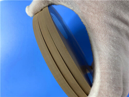
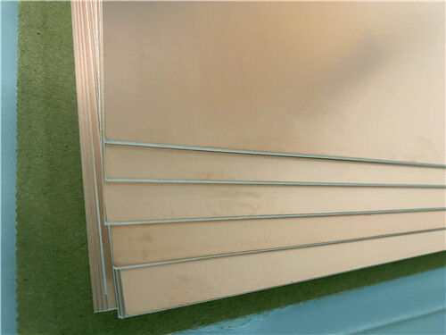
This 2-layer rigid PCB is fabricated using TP2000, a specialized high-frequency thermoplastic material composed of ceramic and polyphenylene oxide (PPO) resin, with no glass fiber reinforcement. It is specifically engineered for high-frequency radio frequency (RF) and microwave applications. TP2000 exhibits an ultra-high dielectric constant (DK), an ultra-low dissipation factor (Df), and superior thermal stability, rendering it highly suitable for designs requiring compact form factors and optimal signal integrity. This PCB features a finished thickness of 6.1mm, 1 oz (1.4 mils) copper cladding on both outer layers, a bare copper surface finish, and undergoes 100% electrical functionality testing prior to shipment, thereby ensuring consistent and reliable performance in high-frequency systems.
PCB Specifications
| Specification Item |
Technical Specification |
| Base Substrate Material |
TP2000 |
| Layer Configuration |
2 Layers (Double-Sided Rigid) |
| Board Dimensions |
85mm x 85mm (per unit), with a dimensional tolerance of ±0.15mm |
| Minimum Trace Width/Space |
6/7 mils |
| Minimum Drill Hole Size |
0.35mm |
| Blind Vias Configuration |
Not Equipped |
| Finished Board Thickness |
6.1mm |
| Finished Copper Weight (Outer Layers) |
1 oz (1.4 mils) |
| Via Plating Thickness |
20 μm |
| Surface Finish |
Bare Copper |
| Top Silkscreen Configuration |
Not Equipped |
| Bottom Silkscreen Configuration |
Not Equipped |
| Top Solder Mask Configuration |
Not Equipped |
| Bottom Solder Mask Configuration |
Not Equipped |
| Electrical Testing Requirements |
100% electrical functionality testing is conducted prior to shipment to ensure operational integrity |
PCB Stack-Up Configuration
This 2-layer rigid PCB adopts a symmetric stack-up structure, with detailed layer specifications provided below (arranged from top to bottom):
| Layer Designation |
Technical Specification |
| Copper Layer 1 (Top) |
35 μm |
| TP2000 Core Substrate |
6 mm |
| Copper Layer 2 (Bottom) |
35 μm |

Artwork Format and Quality Compliance
The Gerber RS-274-X format is officially specified as the artwork standard for this PCB, ensuring seamless compatibility with professional PCB design software and automated manufacturing equipment throughout the entire production workflow. This PCB adheres strictly to the IPC-Class-2 quality standard, which sets forth rigorous requirements for performance, reliability, and manufacturing consistency, thereby confirming its suitability for high-reliability RF and microwave applications.
Global Availability
This high-performance PCB is available for global shipping. It caters to both prototyping needs and large-volume production orders, ensuring convenient accessibility and timely delivery to customers across the globe.
TP2000 Substrate Introduction
TP2000 is a unique high-frequency thermoplastic material in the industry. The dielectric layer of TP-based sheets is made up of ceramic and polyphenylene oxide (PPO) resin, without glass fiber reinforcement, and is specifically designed for high-frequency RF and microwave applications. It boasts an ultra-high dielectric constant, ultra-low dissipation factor, and excellent thermal stability, making it ideal for designs that require compact size and high signal integrity. The material operates reliably over a wide temperature range, is easy to machine, and is compatible with standard PCB fabrication processes.
TP2000 Key Features
| Key Features |
Specifications & Details |
| Dielectric Constant (DK) |
20 at 5GHz |
| Dissipation Factor (Df) |
0.002 at 5GHz |
| Thermal Coefficient of DK (TCDK) |
-55 ppm/°C |
| Coefficient of Thermal Expansion (CTE) |
X=35 ppm/°C, Y=35 ppm/°C, Z=40 ppm/°C |
| Operating Temperature Range |
-100°C to +150°C |
| Mechanical Performance |
High mechanical strength and dimensional stability |
| Radiation Resistance |
Excellent radiation resistance |
| Machinability |
Easy machinability (drilling, cutting, engraving) |
| Assembly Compatibility |
Compatible with standard PCB assembly processes |
| Flammability Rating |
UL 94-V0 |
Typical Applications
- High-frequency RF and microwave circuits
- Antenna systems (including phased array antennas)
- Radar systems (automotive, aerospace, defense)
- Satellite communication equipment
- High-power RF amplifiers
- Test and measurement instruments
- Aerospace and defense electronics
Microwave Composite Dielectric Copper-Clad Substrate TP-1/2 and TP2000
TP material is a unique high-frequency thermoplastic material in the industry. The dielectric layer of TP-series laminates consists of ceramics and polyphenylene (PPO) resin, with no glass fiber reinforcement. The dielectric constant is precisely adjusted by varying the ratio between ceramic and PPO resin. The production process is special, resulting in excellent dielectric performance and high reliability. "TP" refers to the non-clad (uncoppered) smooth surface material, "TP-1" refers to single-sided copper-clad material, and "TP-2" refers to double-sided copper-clad material.
Product Features
- The dielectric constant can be selected within a range of 3 to 25 according to circuit requirements, with stable performance. Commonly available values include 3.0, 4.4, 6.0, 6.15, 9.2, 9.6, 10.2, 11, 16, and 20. Low dielectric loss; loss increases with frequency, but remains relatively stable within 10 GHz.
- Long-term operating temperature range from -100°C to +150°C, with excellent low-temperature performance. When temperatures exceed 180°C, the material may deform, copper foil may detach, and electrical properties may change significantly.
- Minimum thickness of 0.5 mm, with a wide range of thickness options available; custom thicknesses can be accommodated.
- Radiation-resistant and low outgassing.
- Ideal material for BeiDou navigation systems, missile-borne applications, fuzes, and miniaturized antennas.
- Copper foil adhesion to the dielectric is stronger than vacuum-deposited metal films on ceramic substrates. The material is easy to machine and can be drilled, turned, ground, sheared, and milled — capabilities that ceramic substrates cannot match.
- Easy PCB fabrication: can be processed using standard thermoplastic methods, with high yield and significantly lower processing costs compared to ceramic substrates. Due to the material's characteristics, multilayer board processing is generally not recommended. If multilayer processing is necessary, please select low-temperature bonding sheets and carefully evaluate feasibility.
- The material is not suitable for 260°C thermal shock testing and cannot withstand wave soldering. Soldering recommendations: manual soldering with a constant-temperature soldering iron. Reflow soldering is generally not recommended; if reflow soldering is necessary, the maximum set temperature should not exceed 200°C, and feasibility and stability must be thoroughly evaluated.

 Your message must be between 20-3,000 characters!
 English