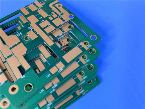
This 4-layer high-frequency hybrid PCB adopts a composite substrate combining RT/duroid 5880 and high Tg FR4, which perfectly balances excellent high-frequency performance and cost-effectiveness. Manufactured in strict compliance with IPC-3 standards, it features precise structural control and reliable process quality, equipped with controlled depth slot technology and high-standard copper plating, making it suitable for high-frequency signal transmission scenarios that require stability and precision.
PCB Specifications
| Specification Item |
Technical Specification |
| Layer Configuration |
4-Layer Rigid PCB (6-layer structure) |
| Base Substrate Material |
RT/duroid 5880 + High Tg FR4 (Hybrid Substrate) |
| Finished Board Thickness |
1.0 mm |
| Board Dimensions |
90mm × 80mm (per unit), 1 piece per unit |
| Copper Weight (Inner Layers) |
0.5 oz |
| Finished Copper Weight |
1 oz |
| Surface Finish |
Immersion Gold (2 U") |
| Solder Mask & Silkscreen |
Blue Solder Mask with White Silkscreen Text |
| Plated Through-Hole (PTH) Copper Thickness |
25 μm |
| Quality Standard |
IPC-3 Compliant |
| Special Process |
Controlled Depth Slot (Depth tolerance is strictly maintained within ±0.05mm with real-time laser ranging feedback; slot wall angle is 85°-90° achieved via mechanical milling). |
PCB Stack-Up Structure (From Top to Bottom)
| Layer/Component |
Thickness |
| L1 Copper (Top Layer) |
0.035 mm |
| RT/duroid 5880 Core |
0.254 mm |
| L2 Copper (Inner Layer 1) |
0.018 mm (0.5 oz) |
| Prepreg |
0.12 mm |
| FR4 Core |
0.1 mm |
| Prepreg |
0.12 mm |
| L3 Copper (Inner Layer 2) |
0.018 mm (0.5 oz) |
| FR4 Core |
0.254 mm |
| L4 Copper (Bottom Layer) |
0.035 mm |

RT/duroid 5880 Substrate Introduction
RT/duroid 5880 is a glass microfiber reinforced PTFE composite material, specifically designed for exacting stripline and microstrip circuit applications. Its randomly oriented microfibers ensure exceptional dielectric constant uniformity, which is consistent from panel to panel and remains stable over a wide frequency range. With a low dissipation factor, it can be applied to Ku-band and above. The material is easy to cut, shear and machine, and resistant to all solvents and reagents (hot or cold) commonly used in PCB etching and plating processes. It is an ideal high-frequency substrate for scenarios requiring stable electrical performance.
Key Features
-Lowest electrical loss among reinforced PTFE materials
-Low moisture absorption, ensuring stable performance in different environments
-Isotropic, with uniform physical and electrical properties in all directions
-Uniform electrical properties over a wide frequency range
-Excellent chemical resistance, compatible with common PCB processing reagents
Application Fields
- Commercial Airline Broadband Antennas
- Microstrip and Stripline Circuits
- Millimeter Wave Applications
- Radar Systems
- Missile Guidance Systems
- Point to Point Digital Radio Antennas
Processing Points
Surface Treatment: After etching, protect the dielectric surface roughness to enhance inner layer bonding; pure PTFE surface requires sodium treatment or plasma treatment to improve adhesion.
Cleaning & Drying: Ensure the board surface is clean and dry before milling; avoid mechanical brushing to prevent surface damage.
Copper Surface Treatment: Select appropriate inner copper surface treatment (such as oxidation) according to the prepreg type, following PTFE multi-layer board processing guidelines.
Machinability: Easy to cut, shear and machine, compatible with standard PCB processing equipment, but needs to control processing parameters to ensure dimensional stability.
Controlled Depth Slot Introduction
Definition
Controlled depth slot is a special PCB processing technology that involves milling a slot with a specific depth on the board surface, without penetrating the entire board thickness. It is mainly used to meet the assembly requirements of components, avoid signal interference, or realize special structural design, ensuring the PCB can be perfectly matched with other components in the electronic device.
Processing Requirements
Depth Tolerance: Strictly controlled within ±0.05mm, with real-time laser ranging feedback to ensure precision.
Slot Wall Angle: Maintained at 85°-90° through mechanical milling, ensuring the slot wall is flat and smooth, meeting assembly and signal transmission requirements.
Processing Precision: High precision milling equipment is required to avoid slot edge burring, uneven depth, and other defects that affect product performance.
Application Significance
The controlled depth slot technology effectively solves the problem of component assembly interference and signal crosstalk in high-frequency PCBs. It ensures the compact structure of the PCB, improves the integration of the device, and at the same time maintains the structural strength of the board, ensuring the stability and reliability of the product in long-term operation.

 Your message must be between 20-3,000 characters!
 English