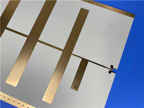
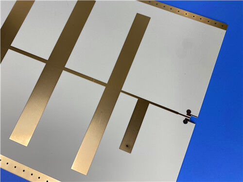
This 2-layer rigid WL-CT615 high-frequency PCB delivers high-stability, cost-efficient RF performance for modern communication infrastructure, automotive radar units, and satellite antenna systems. Built with Wangling advanced WL-CT615 organic polymer ceramic fiberglass laminate, this thermosetting substrate features minimized high-frequency signal attenuation and superior thermal stability. It offers simpler fabrication processes and higher circuit consistency than traditional PTFE materials, supporting large-volume commercial production. Engineered with an ultra-thin 0.3mm finished thickness and 1oz outer copper weight, the PCB adopts premium ENEPIG surface finishing to ensure robust solderability, long-term oxidation resistance, and reliable operational performance. It supports 4/5 mil fine-line trace and spacing alongside 0.4mm minimal mechanical drilling, with a non-blind via structure for stable signal routing. Dual-sided green solder mask provides full circuit protection, while double-sided white silkscreen enables clear component marking and assembly convenience.
PCB Specification
| Specification Item |
Details |
| Base Material |
Wangling WL-CT615 organic polymer ceramic fiberglass high-frequency laminate |
| Layer Configuration |
2 layers rigid PCB structure |
| Finished Board Thickness |
0.3mm |
| Board Dimension |
99.03mm × 45.6mm (1PCS), dimensional tolerance: ±0.15mm |
| Outer Copper Thickness |
1 oz (1.4 mils) finished copper weight for outer layers |
| Via Plating Thickness |
20 μm plating thickness |
| Minimum Trace/Space |
4/5 mils |
| Minimum Drilling Hole Size |
0.4mm |
| Blind Vias Structure |
Not equipped |
| Surface Finishing |
ENEPIG |
| Silkscreen Printing |
White silkscreen on top and bottom sides |
| Solder Mask Coating |
Green solder mask on top and bottom sides |
| Quality Standard |
IPC-Class-2 industrial specification |
| Pre-Shipment Test |
100% full electrical performance inspection |
PCB Stack-up Structure
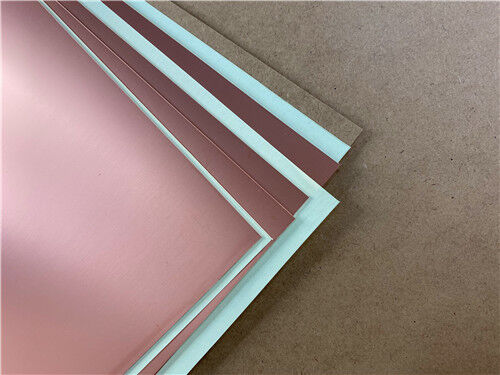
This 2-layer rigid stackup adopts a 0.203mm (8mil) WL-CT615 composite core blended with hydrocarbon resin, ceramic fillers and fiberglass cloth. It features stable dielectric performance, low thermal expansion and outstanding heat resistance. Equipped with dual 35μm high-purity copper layers for uniform signal conduction, this structure supports standard FR4 fabrication, delivering superior manufacturing stability and batch consistency over traditional PTFE high-frequency PCBs.
| Stack-up Layer |
Parameter Details |
| Top Copper Layer |
35 μm thick high-purity copper foil |
| WL-CT615 Dielectric Core |
0.203mm (8mil) organic polymer ceramic fiberglass composite substrate |
| Bottom Copper Layer |
35 μm thick high-purity copper foil |

PCB Statistic
This WL-CT615 high-frequency PCB features optimized component layout and evenly distributed vias. Its well-matched pad configuration and streamlined circuit networking adapt perfectly to compact RF device assembly, sustaining low-loss, interference-free signal transmission for diverse communication and radar modules.
| Statistical Item |
Quantity |
| Mounted Components |
31 |
| Total Pad Count |
69 |
| Through-Hole Pads |
41 |
| Top SMT Pads |
28 |
| Bottom SMT Pads |
0 |
| Via Quantity |
56 |
| Net Circuit Count |
2 |
WL-CT615 Material Overview
WL-CT615 is a high-performance thermosetting copper-clad laminate independently developed by Wangling, formulated with hydrocarbon resin, composite ceramics and fiberglass reinforcement. Unlike PTFE substrates that require complex manufacturing procedures, this material supports mature FR4 processing techniques, greatly improving production efficiency and circuit repeatability. Its unique resin-ceramic composite structure achieves ultra-low high-frequency loss, excellent thermal endurance, and stable dielectric temperature performance. With a high TG value above 280°C, low thermal expansion and ultra-low moisture absorption, WL-CT615 acts as a reliable, cost-effective alternative to imported high-frequency laminates for mainstream RF and microwave applications.
Core Performance Features
WL-CT615 integrates outstanding electrical stability, thermal performance and structural durability, maintaining consistent low-loss signal output under high-frequency operation and variable temperature environments:
| Performance Parameter |
Technical Value & Performance Description |
| Stable Dielectric Constant |
Dk of 6.15 @ 10GHz / 23°C, enabling precise impedance control for stable high-frequency microwave transmission |
| Minimal High-Frequency Loss |
Ultra-low dissipation factor of 0.004 @ 10GHz, minimizes signal attenuation and preserves full signal integrity |
| Suppressed Temperature Drift |
TCDK of -122 ppm/°C, stabilizes dielectric properties amid frequent temperature fluctuations |
| Superior Thermal Conductivity |
0.72 W/MK thermal conductivity, accelerates heat dissipation and improves long-term stability for high-power RF modules |
| Ultra-Low Moisture Absorption |
Only 0.04% moisture absorption rate, prevents electrical parameter drift in humid environments |
| Copper-Matched Thermal Expansion |
X-axis: 15 ppm/°C, Y-axis: 17 ppm/°C, Z-axis: 33 ppm/°C, effectively prevents layer delamination and thermal deformation |
| Excellent Heat Resistance |
TG value over 280°C, delivers reliable thermal stability for high-temperature and high-power operating conditions |
Typical Application Scenarios
Thanks to its ultra-low high-frequency loss, outstanding thermal stability and FR4-compatible processing advantages, WL-CT615 high-frequency PCBs are widely deployed in commercial communication systems, automotive electronic devices and satellite microwave facilities:
- Cellular base station antennas, satellite antennas, WiMAX systems and distributed antenna networks
- Automotive high-frequency radar, precision sensing units and vehicle navigation systems
- High-reliability RF power amplifier modules
- Satellite high-frequency transceiver front-end modules
- RF processing components, high-frequency filters and microwave functional modules
Quality Assurance & Global Service
All WL-CT615 high-frequency circuit boards are manufactured in full compliance with IPC-Class-2 industrial quality standards. Produced with standard Gerber RS-274-X manufacturing files, each PCB maintains precise dimensional accuracy and consistent electrical repeatability for stable mass production. Every finished unit undergoes comprehensive electrical testing prior to delivery to eliminate functional defects and ensure uniform batch quality. Supported by global logistics networks and professional technical teams, we deliver dependable high-frequency PCB solutions for worldwide communication, automotive and satellite microwave projects.


 Your message must be between 20-3,000 characters!
 English