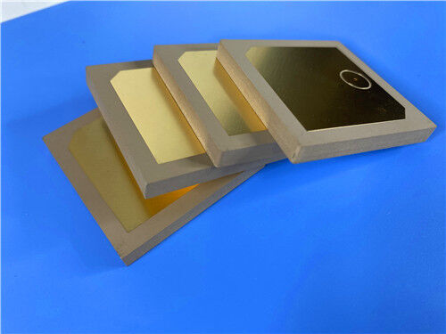
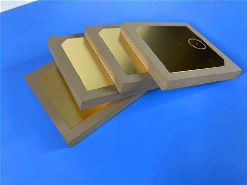
Tailored for high-reliability miniaturized RF and precision navigation applications, this custom 2-layer rigid PCB adopts premium Wangling TP2200 thermoplastic PPO ceramic substrate. Boasting an ultra-thick 10.9mm finished board thickness and a 35.65mm × 87mm dimensional footprint with strict ±0.15mm tolerance, the board features pure immersion gold surface finishing, with no solder mask or silkscreen layered on either side. Built with a full through-hole structure and zero blind vias, it supports precise 4/7 mil minimum trace/space routing and 0.4mm micro-hole fabrication to adapt to compact high-density circuit layout demands. Every unit undergoes 100% comprehensive electrical testing prior to shipment, complies with IPC-Class-2 industrial quality standards, and supports stable worldwide supply and customized services for specialized high-frequency electronic projects.
PCB Specifications
Engineered with industry-unique thermoplastic dielectric structure, this TP2200 2-layer PCB delivers exceptional dielectric stability and mechanical robustness for high-Dk RF circuit design. Eliminating glass fiber reinforcement interference, its standardized fabrication parameters ensure consistent signal transmission performance and long-term operational reliability in extreme working environments.
| Specification Item |
Parameter Details |
| Base Material |
Wangling TP2200 thermoplastic PPO ceramic substrate |
| Layer Configuration |
2-layer rigid PCB |
| Board Dimensions |
35.65mm × 87mm (±0.15mm tolerance, 1PCS) |
| Minimum Trace / Space |
4/7 mils |
| Minimum Hole Size |
0.4mm |
| Via Type |
Through-hole only, no blind vias |
| Finished Board Thickness |
10.9mm |
| Outer Copper Weight |
1oz (1.4 mils) |
| Via Plating Thickness |
20μm |
| Surface Finish |
Immersion Gold |
| Silkscreen |
Top & Bottom: No |
| Solder Mask |
Top & Bottom: No |
| Pre-Shipment Test |
100% electrical test prior to shipment |
PCB Stack-up Structure
This 2-layer PCB adopts a symmetrical and compact stackup layout, centered on a 0.8mm Wangling TP2200 core dielectric substrate. Double-sided 35μm pure copper layers are evenly laminated on both sides of the core, forming a balanced structural design. This rational stackup configuration delivers uniform thermal conductivity and stable dielectric performance, effectively avoiding signal deviation and structural deformation under extreme temperature conditions.
| Layer Structure |
Material & Thickness |
| Copper_layer_1 |
35 μm |
| TP2200 Core |
0.8 mm |
| Copper_layer_2 |
35 μm |
PCB Statistic
Optimized for miniaturized high-frequency circuit assembly, this PCB features a streamlined layout with 34 integrated components and scientific distribution of pads and vias, perfectly matching high-Dk compact circuit design requirements. All production design files are provided in standard Gerber RS-274-X format, ensuring full compatibility with mainstream PCB manufacturing and testing equipment for precise prototyping and stable batch production.
| Statistical Item |
Quantity |
| Components |
34 |
| Total Pads |
29 |
| Thru Hole Pads |
22 |
| Top SMT Pads |
7 |
| Bottom SMT Pads |
0 |
| Vias |
16 |
| Nets |
1 |

Introduction of Wangling TP Series Material
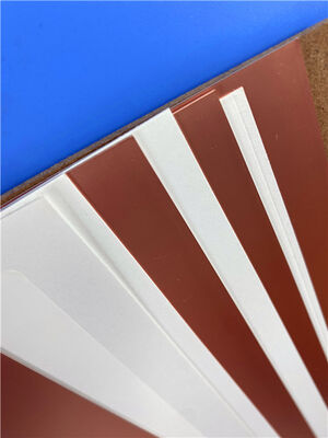
The Wangling TP series represents a distinctive high-frequency thermoplastic substrate solution in the industry. Its dielectric layer is formulated with ceramic filler and polyphenylene oxide (PPO) resin, completely free of woven glass fabric reinforcement to eliminate glass weave signal interference. Engineers can precisely adjust the dielectric constant by modifying the mixing ratio of ceramic and PPO resin, realizing customized dielectric performance for diverse circuit designs. Manufactured via exclusive specialized processes, the TP series delivers excellent dielectric stability and superior long-term reliability. For product specification definition, TP stands for unclad smooth substrate, TP-1 for single-sided copper clad laminate, and TP-2 for double-sided copper clad laminate.
Core Performance Features of TP2200
TP2200 is a high-Dk thermoplastic ceramic substrate tailored for extreme-environment high-frequency applications. It integrates ultra-low dielectric loss, outstanding temperature resistance and exceptional structural stability, making it irreplaceable for miniaturized navigation and special military RF equipment:
| Performance Parameter |
Specification |
| Dielectric Constant (Dk @5GHz) |
22 ± 0.88 |
| Dissipation Factor (Df @5GHz) |
0.002 ~ 0.0025 |
| Thermal Coefficient of Dk (TCDK) |
-55 ppm/℃ |
| CTE (X/Y/Z Axis) |
35ppm/℃, 35ppm/℃, 40ppm/℃ |
| Long-term Operating Temperature |
-100°C to +150°C |
| Water Absorption |
≤0.01% |
| Thermal Conductivity |
0.9W/MK |
| Special Material Properties |
Radiation resistance, low outgassing |
Typical Applications
Benefiting from its ultra-high Dk value, ultra-low water absorption, extreme temperature adaptability and radiation-resistant performance, this TP2200 2-layer PCB is widely applied in high-precision, high-reliability special RF and navigation fields:
- Beidou navigation systems
- Missile-borne electronic equipment
- Precision fuzes
- Miniaturized high-frequency antennas
Conclusion
Featuring premium immersion gold surface treatment and a robust 10.9mm thick body, this custom Wangling TP2200 PCB delivers high-Dk, low-loss and thermally stable performance for extreme-environment high-frequency applications. Its glass-free PPO ceramic structure, ultra-low water absorption, excellent radiation resistance and wide temperature tolerance enable stable operation in military, navigation and precision antenna scenarios. Fully inspected with 100% electrical testing and certified to IPC-Class-2 standards, this PCB provides reliable customized solutions and global delivery for specialized high-frequency electronic engineering projects worldwide.


 Your message must be between 20-3,000 characters!
 English