|
Product Details:
|
| Base Material: | TFA300 | Layer Count: | Single Side |
|---|---|---|---|
| PCB Thickness: | 0.2mm | PCB Size: | 87mm × 54mm (±0.15mm Tolerance Per Piece) |
| Solder Mask: | Green | Silkscreen: | No |
| Copper Weight: | 1oz (1.4 Mils) Outer Layers | Surface Finish: | Immersion Gold |
| Highlight: | Flexible Printed FPC Circuit Board,Single Sided Polyimide FPC Circuit Board,Telemetry System FPC Circuit Board |
||
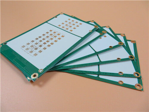
This TFA300 2-layer rigid PCB is a premium high-frequency printed circuit board tailored for aerospace, microwave communication, and radar system applications. This high-reliability PCB features a 0.2mm finished board thickness, premium immersion gold surface finish, and 1oz outer layer copper weight, paired with a precise 2-layer rigid stackup built on high-performance TFA300 PTFE ceramic composite substrate. Manufactured to strict IPC-Class-2 quality standards and fully verified with 100% electrical testing before shipment, it delivers outstanding frequency stability, ultra-low dielectric loss, and reliable thermal mechanical performance. Adopting a unique glass-fiber-free formula that eliminates traditional fiberglass electromagnetic interference, this PCB acts as a cost-effective, high-quality alternative to imported high-frequency PCB substrates and supports worldwide supply and professional technical services.
What Is TFA300 Substrate?
The TFA series is a cutting-edge Polytetrafluoroethylene (PTFE) ceramic composite dielectric substrate, featuring a unique production process that differs fundamentally from traditional glass fiber cloth prepreg manufacturing. Instead of resin-impregnated fiberglass fabric, it adopts uniform nano-ceramic and resin composite mixing technology, paired with professional customized lamination pressing procedures to produce high-performance PCB core materials.
Eliminating the fiberglass effect during electromagnetic wave transmission, the TFA series effectively avoids signal distortion and frequency deviation, achieving outstanding electromagnetic stability. It features minimized X/Y/Z axis anisotropy, ultra-low thermal expansion coefficient matching copper foil, and stable dielectric temperature characteristics, ensuring consistent performance in extreme temperature environments. The TFA substrate family offers four customizable dielectric constant options: 2.94 (TFA294), 3.0 (TFA300), 6.15 (TFA615), and 10.2 (TFA1020), covering diverse high-frequency circuit design requirements.
![]()
Why Choose TFA300 PCB? Core High-Frequency Performance Features
The TFA300 substrate is the mainstream high-frequency grade of the TFA series, with stable and superior electrical, thermal, and physical properties, fully meeting aerospace-grade high-reliability application standards:
Stable Dielectric Constant (Dk): 3.0±0.04 at 10GHz, ensuring consistent high-frequency signal transmission
Ultra-Low Dissipation Factor (Df): 0.001 at 10GHz and 20GHz, 0.0012 at 40GHz, effectively reducing high-frequency signal attenuation
Excellent Temperature Stability: Low TCDK of -8 ppm/°C within -55°C to 150°C, maintaining stable dielectric performance under temperature fluctuations
Balanced Thermal Expansion Coefficient (CTE): 18 ppm/°C (X-axis), 18 ppm/°C (Y-axis), 30 ppm/°C (Z-axis) in -55°C to 288°C, perfectly matching copper foil expansion and contraction to prevent board cracking and circuit failure
Superior Thermal Conductivity: 0.6 W/mk, accelerating heat dissipation and improving circuit operating stability
Low Moisture Absorption: 0.04% moisture absorption rate, avoiding performance degradation caused by humid environments
Flame Retardant Rating: UL 94-V0 grade, meeting global safety and fire resistance standards for electronic equipment
Key PCB Specification
| Parameter Item | Specific Specification |
| Base Material | TFA300 high-frequency ceramic PTFE composite substrate |
| Layer Count | 2 layers (rigid structure) |
| Board Dimensions | 87mm × 54mm (±0.15mm tolerance per piece) |
| Minimum Trace/Space | 6/8 mils, supporting fine-line circuit design |
| Minimum Hole Size | 0.4mm |
| Via Design | No blind vias, only through-hole vias for enhanced structural stability |
| Finished Board Thickness | 0.2mm, ultra-thin and lightweight for compact device integration |
| Finished Copper Weight | 1oz (1.4 mils) outer copper layers, ensuring excellent conductivity and current carrying capacity |
| Via Plating Thickness | 20μm, guaranteeing reliable via conductivity and oxidation resistance |
| Surface Finish | Immersion gold, optimizing soldering performance and component adhesion |
| Silkscreen | No top and bottom silkscreen, meeting high-frequency signal transmission purity requirements |
| Solder Mask | Green top solder mask, no bottom solder mask |
| Quality Test | 100% full electrical testing before shipment to eliminate circuit open/short defects |
2-Layer High-Frequency Optimized Stack-up Structure
The standardized layered structure ensures uniform stress distribution and stable high-frequency performance:
| Layer Sequence | Material Specification | Thickness | Core Function |
| Outer Layer 1 (Top) | Conductive Copper Foil | 35μm | High-frequency signal transmission, component soldering pad carrier |
| Core Dielectric Layer | TFA300 High-Frequency Ceramic PTFE Composite Substrate | 0.127mm (5mil) | Stable dielectric support, low-loss high-frequency signal isolation |
| Outer Layer 2 (Bottom) | Conductive Copper Foil | 35μm | Circuit signal transmission, structural support balance |
PCB Statistics
| Parameter Item | Specific Value |
| Components | 18 |
| Total Pads | 36 |
| Thru Hole Pads | 19 |
| Top SMT Pads | 17 |
| Bottom SMT Pads | 0 |
| Vias | 6 |
| Nets | 2 |
![]()
Accepted Artwork Format: We accept standard Gerber RS-274-X files submitted by global customers. This industry-standard file format is used for accurate technical evaluation, formal quotation confirmation, and official mass production, enabling efficient and error-free project communication and manufacturing docking worldwide.
Production Quality Standard: All PCBs are strictly manufactured and inspected in compliance with IPC-Class-2 industrial reliability standards. This standardized quality control ensures stable, consistent, and reliable circuit performance, fully meeting the requirements of commercial, industrial, and aerospace high-frequency application scenarios.
Global Supply Service: We provide global customized PCB quotation services and worldwide shipping support. Customers from all regions of the world can submit Gerber files for personalized PCB quotation, and we offer a complete one-stop solution including engineering technology confirmation, precision production, full inspection, and international delivery.
Typical Usage Scenarios
Benefiting from its aerospace-grade high-frequency performance, low signal loss, and extreme environmental adaptability, this TFA300 PCB is widely applied in high-precision wireless communication and radar detection fields:
Aerospace & Aviation: Aerospace equipment, space devices, aircraft cabin electronic systems, airborne precision modules
Microwave & Antenna Systems: Microwave signal transmission modules, high-precision antennas, phase-sensitive antenna equipment
Radar Detection: Early warning radar systems, airborne radar modules, high-frequency radar detection equipment
Phased Array Systems: Phased array antennas, beamforming network circuit boards
Satellite Communication & Navigation: Satellite communication terminals, navigation positioning system modules
Radio Frequency Devices: High-frequency power amplifiers and RF signal processing circuits
![]()
Contact Person: Ms. Ivy Deng
Tel: 86-755-27374946
Fax: 86-755-27374848