logo
Home ProductsF4B PCB

2-layer F4BTMS265 PCB 30mil High-Frequency Substrate

Certification
China Bicheng Electronics Technology Co., Ltd certification
Customer Reviews
Kevin, Received and tested the boards - thanks very much. These are perfect, exactly what we needed. rgds Rich

—— Rich Rickett

Ruth, I got the PCB today, and they are just perfect. Please stay a little patience, my next order is coming soon. Kind regards from Hamburg Olaf

—— Olaf Kühnhold

Hi Natalie. It was perfect, I attach some pictures for your reference. And I send you next 2 projects to budget. Thanks a lot again

—— Sebastian Toplisek

Kevin, Thanks, they were perfectly made, and work well. As promised, here are the links for my latest project, using the PCBs you manufactured for me: Regards, Daniel

—— Daniel Ford

I'm Online Chat Now

2-layer F4BTMS265 PCB 30mil High-Frequency Substrate

2-layer F4BTMS265 PCB 30mil High-Frequency Substrate
2-layer F4BTMS265 PCB 30mil High-Frequency Substrate 2-layer F4BTMS265 PCB 30mil High-Frequency Substrate

Large Image :  2-layer F4BTMS265 PCB 30mil High-Frequency Substrate

Product Details:
Place of Origin: CHINA
Brand Name: Bicheng
Certification: UL, ISO9001, IATF16949
Model Number: BIC-268.V1.0
Payment & Shipping Terms:
Minimum Order Quantity: 1PCS
Price: USD9.99-99.99
Packaging Details: Vacuum bags+Cartons
Delivery Time: 8-9 working days
Payment Terms: T/T
Supply Ability: 5000PCS per month

2-layer F4BTMS265 PCB 30mil High-Frequency Substrate

Description
Base Material: F4BTMS265 Layer Count: 2 Layers
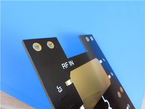
PCB Thickness: 0.85mm PCB Size: 97mm × 76mm (1 Piece), Dimensional Tolerance: ±0.15mm
Solder Mask: Black Silkscreen: White
Copper Weight: 1oz (1.4 Mils) Outer Copper Layer Surface Finish: ENIG (Electroless Nickel Immersion Gold)
Highlight:

Polyimide Stiffener 4 Layer Flex PCB

,

2 Oz Copper 4 Layer Flex PCB

,

Polyimide Stiffener 2 Oz Copper PCB

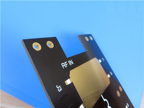
This 2-layer rigid high-frequency PCB features aerospace-grade F4BTMS265 ceramic-filled dielectric substrate with low electromagnetic loss and minimal anisotropy. It adopts ENIG surface treatment, black top solder mask and white top silkscreen, with a fully mask-free and silkscreen-free bottom side. All units pass 100% electrical testing before delivery, ensuring stable dielectric performance, low signal attenuation and reliable structure for aerospace, military and RF/microwave applications.


PCB Specifications

Parameter Item Specification
Base Material F4BTMS265 upgraded ceramic-filled high-frequency substrate
Layer Configuration 2-layer rigid PCB structure
Board Dimension 97mm × 76mm (1 piece), dimensional tolerance: ±0.15mm
Minimum Trace / Space 14 mils / 14 mils
Minimum Mechanical Hole Diameter 0.25mm
Via Type Pure through-hole vias, no blind vias
Finished Board Thickness 0.85mm
Outer Copper Weight 1oz (1.4 mils) outer copper layer
Via Plating Thickness 20μm
Surface Finishing ENIG (Electroless Nickel Immersion Gold)
Top Silkscreen White silkscreen
Bottom Silkscreen Silkscreen-free
Top Solder Mask Black solder mask
Bottom Solder Mask Solder mask-free
Quality Inspection 100% full electrical testing performed prior to delivery


PCB Layer Stack-up Structure

Layer Definition Technical Specification
Top Copper Layer 35μm finished copper thickness
Dielectric Core Substrate F4BTMS265 core, 0.762mm (30mil) thickness
Bottom Copper Layer 35μm finished copper thickness


2-layer F4BTMS265 PCB 30mil High-Frequency Substrate 0


Artwork & Quality Compliance

Production File Standard: Fabricated based on industry-standard Gerber RS-274-X files, supporting high-precision circuit patterning and full compatibility with mainstream industrial manufacturing processes.


Quality Standard: All fabrication and inspection procedures comply strictly with IPC-Class-2 specifications, ensuring stable electrical performance and long-term structural reliability.


Global Availability: Worldwide supply and logistics services are available to support global aerospace and high-frequency electronic projects.


F4BTMS265 Material Profile

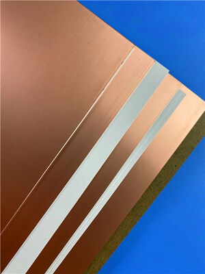
F4BTMS265 is an upgraded high-reliability ceramic-reinforced PTFE dielectric substrate optimized from the standard F4BTM series. Filled with uniformly distributed nano-ceramic particles and ultra-fine glass fiber, it reduces glass fiber-caused electromagnetic interference, dielectric loss and structural anisotropy. Adopting low-roughness RTF copper foil as standard, it delivers low conductor loss and stable peel strength, and supports copper/aluminum base lamination. With excellent dimensional, thermal and dielectric stability, this aerospace-grade material serves as a high-performance substitute for imported high-frequency substrates in military and aerospace applications.


2-layer F4BTMS265 PCB 30mil High-Frequency Substrate 1


Typical Application Fields

Featuring ultra-low dielectric loss, minimal structural anisotropy, superior thermal stability and aerospace-grade reliability, F4BTMS265-based PCBs are well-suited for deployment in high-precision, phase-sensitive high-frequency electronic systems:


  • Aerospace devices, space equipment and cabin electronic systems
  • High-frequency RF and microwave circuit systems
  • High-precision military radar equipment
  • Antenna feed network components
  • Phase-sensitive antennas and phased array antenna systems
  • Satellite communication systems

2-layer F4BTMS265 PCB 30mil High-Frequency Substrate 2


Contact Details
Bicheng Electronics Technology Co., Ltd

Contact Person: Ms. Ivy Deng

Tel: 86-755-27374946

Fax: 86-755-27374848

Send your inquiry directly to us (0 / 3000)