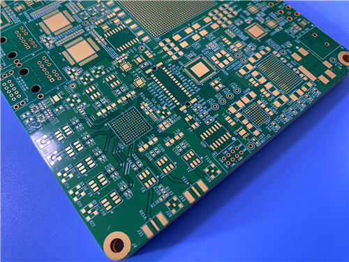
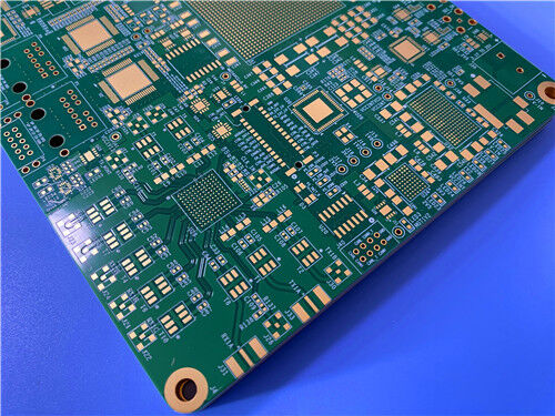
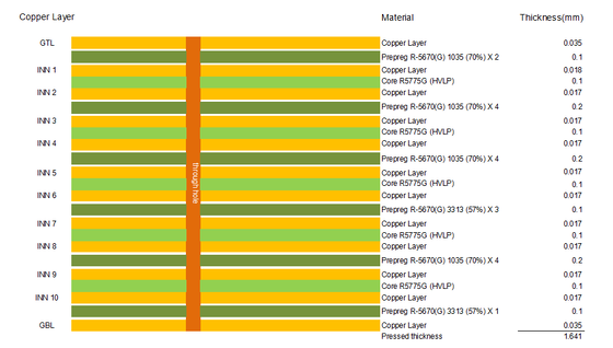
14-Layer Megtron 6 High-Speed PCB is an ultra-low loss high-reliability multilayer circuit board ideal for high-speed networking, mobile communication and high-density HDI electronic systems. Adopting premium Panasonic Megtron 6 ultra-low loss substrate, this 14-layer PCB delivers outstanding dielectric stability, superior thermal resistance and precise impedance control performance. It fully complies with strict IPC-3 industrial standards to support high-frequency and high-speed signal transmission with minimal latency and signal attenuation.
This custom high-speed PCB adopts differentiated copper thickness configuration:1oz outer copper layers for stable high-current conduction and reliable soldering performance, and 0.5oz inner copper layers for fine-line routing and high-density layout. The finished board thickness is 1.64mm, with a single size of 178.8×169mm. The product ships in a 2×2 panel combination (4 pieces total), with 5mm width process edges reserved on all four sides. Featured with green solder mask and white silkscreen plus premium nickel-palladium-gold surface finish, the board ensures excellent oxidation resistance and stable solderability. It adopts IPC-4761 TYPE VII standard resin plugging technology and professional microstrip/stripline impedance matching, meeting high-standard high-speed PCB batch production and long-term reliable operation requirements.
Precise Impedance Control Parameters
This 14-layer Megtron 6 PCB implements strict microstrip and stripline impedance control for single-ended and differential signals, eliminating high-speed signal reflection, crosstalk and waveform distortion to ensure complete signal integrity:
| Impedance Type |
Target Impedance |
Line Width |
Line Spacing |
| Microstrip |
50Ω |
0.2mm |
- |
| Microstrip |
100Ω (Differential) |
0.1mm |
0.101mm |
| Stripline |
50Ω |
0.1mm |
- |
| Stripline |
100Ω (Differential) |
0.2mm |
0.102mm |
14-Layer Megtron 6 PCB Specifications
| Parameter Item |
Detailed Specification |
| PCB Layer Count |
14-layer ultra-low loss high-speed PCB |
| Base Material |
Panasonic Megtron 6 high-speed low-loss substrate |
| Finished Board Thickness |
1.64mm |
| Copper Thickness |
Outer layer: 1oz; Inner layer: 0.5oz |
| Surface Treatment |
Nickel Palladium Gold plating |
| Solder Mask & Silkscreen |
Green solder mask with white silkscreen |
| Board Dimension & Shipment |
178.8×169mm, 4PCS (2×2 panel), 5mm four-sided process edges |
| Core Processes |
IPC-4761 TYPE VII resin plugging, precise microstrip/stripline impedance control |
| Quality Standard |
IPC-3 industrial high-reliability standard |

What Is Megtron 6? Ultra-Low Loss High-Speed PCB Material
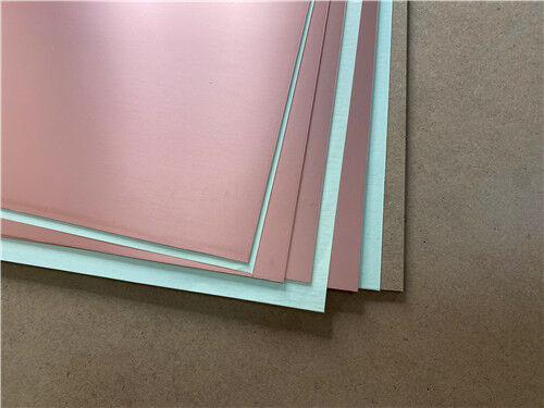
Megtron 6 is a premium ultra-low loss high-speed PCB substrate, serving as the industry standard material for high-frequency, high-speed digital and HDI multilayer circuit designs. Equipped with low Dk glass cloth (R-5775) and matched prepreg (R-5670), Megtron 6 features extremely stable dielectric performance across broadband frequency bands, perfectly catering to high-speed signal transmission demands for networking, mobile communication and wireless devices.
With ultra-low dielectric constant and dissipation factor, Megtron 6 effectively reduces high-speed signal loss and transmission latency. It delivers excellent thermal stability, low thermal expansion coefficient and superior moisture resistance, maintaining stable physical and electrical properties under high-temperature soldering and long-term high-load operation. Supporting HDI high-density interconnection design and standard industrial processing workflows, Megtron 6 is the preferred substrate for high-end high-speed multilayer PCB applications.
| Part Number |
R-5775(K)/R-5670(K) |
R-5775(N)/R-5670(N) |
R-5775(G)/R-5775(G) |
| Tg (DSC) |
185 °C |
185 °C |
185 °C |
| Tg (DMA) |
210 °C |
210 °C |
210°C |
| Td (Thermal Decomposition) (°C) |
410 °C |
410 °C |
410 °C |
| T288 (Without Cu) (min) |
>120 min |
>120 min |
>120 min |
| T288 (With Cu) (min) |
>120 min |
>120 min |
>120 min |
| CTE-Y |
14-16 ppm/°C |
14-16 ppm/°C |
14-16 ppm/°C |
| CTE-Y |
14-16 ppm/°C |
14-16 ppm/°C |
14-16 ppm/°C |
| CTE-Z |
45 ppm/°C |
45 ppm/°C |
45 ppm/°C |
| CTE α2 Z-axis: Test Method IPC-TM-650 2.4.24; Condition A (ppm/℃) |
260 ppm/°C |
260 ppm/°C |
260 ppm/°C |
| Thermal Conductivity, (W/m・K) |
0.42 W/m · K |
0.42 W/m · cm |
0.42 W/m · cm |
| Volume Resistivity (MΩ・cm) |
1 x 10⁹ MΩ · cm |
1 x 10⁹ MΩ · cm |
1 x 10⁹ MΩ · cm |
| Surface Resistivity (mΩ) |
1 x 10⁸ MΩ |
1 x 10⁸ MΩ |
1 x 10⁸ MΩ |
| Dielectric Constant (Dk) @ 1Ghz; Test Method IPC-TM-650; Condition C-24/23/50 |
3.4 |
3.4 |
3.4 |
| Dielectric Constant (Dk) @ 10Ghz; Test Method IPC-TM-650; Condition C-24/23/50 |
—— |
—— |
—— |
| Dielectric Constant (Dk) @ 12Ghz; Test Method Balanced-type Circular Disk Resonator; Condition C-24/23/50 |
3.4 |
3.4 |
3.4 |
| Df at 1 GHz |
0.002 |
0.002 |
0.002 |
| Df at 10 GHz |
—— |
—— |
—— |
| Df at 12 GHz |
0.004 |
0.004 |
0.004 |
| Water Absorption (%) |
0.14% |
0.14% |
0.14% |
| Poisson's Ratio |
0.2 |
0.2 |
0.2 |
| Flexural Warp (MD) (GPa) |
19 GPa |
19 GPa |
19 GPa |
| Flexural Fill (TD) (GPa) |
18 GPa |
18 GPa |
18 GPa |
| Peel Strength (1 Oz. Cu) (kN/m) |
0.8 (Cu:H-VLP) kN/m |
0.8 (Cu:H-VLP) kN/m |
0.8 (Cu:H-VLP) kN/m |
| Flammability |
94V-0 |
94V-0 |
94V-0 |
Megtron 6 Processing & Storage Guidelines
Megtron 6 laminates and prepregs require standardized storage and processing procedures to retain optimal ultra-low loss performance and structural stability. Flat storage in a cool and dry environment is mandatory to avoid bending and surface scratching. Prepreg needs storage conditions below 23℃ and 50% RH, with long-term storage at 5℃ low temperature. Exposed prepreg cumulative open-air time cannot exceed 8 hours to prevent moisture absorption and performance attenuation.
Inner layers adopt professional chemical cleaning and oxide treatment. Peroxide/sulfuric acid organic coating treatment is preferred to ensure stable interlayer bonding strength. Complete moisture removal drying treatment at 105℃ for 20-30 minutes effectively eliminates surface and internal moisture, ensuring high lamination quality and long-term PCB reliability.
Megtron 6 PCB Application Fields
High-Speed Networking Equipment: Core router boards, network switch mainboards and high-speed signal transmission modules
Mobile & Wireless Communication: 5G/6G wireless terminal equipment, high-frequency signal processing circuit boards
High-Density HDI Devices: Multilayer HDI circuit boards requiring miniaturization and high-reliability performance
High-Performance Computing: Server high-speed backplanes, data storage and high-speed computing modules
Conclusion
This 14-layer Megtron 6 high-speed PCB is a high-end ultra-low loss multilayer circuit solution for high-speed digital and communication systems. Equipped with precise microstrip and stripline impedance control, dual copper thickness design and reliable nickel-palladium-gold surface finish, this 1.64mm thick PCB delivers ultra-stable high-speed signal integrity and long-term operational reliability. It is the ideal choice for high-end networking, wireless communication and high-performance computing high-speed PCB customization projects.


 Your message must be between 20-3,000 characters!
 English