logo
Home ProductsRF PCB Board

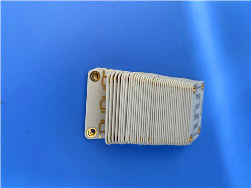
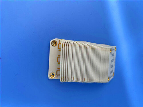
2-layer AD300D PCB 40mil Thick with EPIG Finish

Certification
China Bicheng Electronics Technology Co., Ltd certification
Customer Reviews
Kevin, Received and tested the boards - thanks very much. These are perfect, exactly what we needed. rgds Rich

—— Rich Rickett

Ruth, I got the PCB today, and they are just perfect. Please stay a little patience, my next order is coming soon. Kind regards from Hamburg Olaf

—— Olaf Kühnhold

Hi Natalie. It was perfect, I attach some pictures for your reference. And I send you next 2 projects to budget. Thanks a lot again

—— Sebastian Toplisek

Kevin, Thanks, they were perfectly made, and work well. As promised, here are the links for my latest project, using the PCBs you manufactured for me: Regards, Daniel

—— Daniel Ford

I'm Online Chat Now

2-layer AD300D PCB 40mil Thick with EPIG Finish

2-layer AD300D PCB 40mil Thick with EPIG Finish

Large Image :  2-layer AD300D PCB 40mil Thick with EPIG Finish

Product Details:
Place of Origin: CHINA
Brand Name: Bicheng
Certification: UL, ISO9001, IATF16949
Model Number: BIC-200.V1.0
Payment & Shipping Terms:
Minimum Order Quantity: 1PCS
Price: USD9.99-99.99
Packaging Details: Vacuum bags+Cartons
Delivery Time: 8-9 working days
Payment Terms: T/T
Supply Ability: 5000PCS per month

2-layer AD300D PCB 40mil Thick with EPIG Finish

Description
Base Material: AD300D Layer Count: Double Sided
PCB Thickness: 1.2mm PCB Size: 67mm X 102.6mm Per Unit, +/- 0.15mm
Copper Weight: 1 Oz Surface Finish: EPIG (nickel Free)
Highlight:

2-layer RF PCB board

,

40mil thick PCB board

,

EPIG finish PCB board

This double-sided PCB utilizes AD300D as its core substrate and incorporates an EPIG (nickel-free) surface finish. Configured with 1oz (1.4 mils) copper cladding on the outer layers, a finished board thickness of 1.2mm, and 20 μm via plating, the PCB delivers consistent electrical performance and high-precision manufacturing uniformity, making it highly suitable for applications including cellular infrastructure base station antennas, automotive telematics antenna systems, and commercial satellite radio antennas.


PCB Construction Details

Specifications Details
Base material AD300D
Layer count Double sided PCB
Board dimensions 67mm x 102.6mm per unit, +/- 0.15mm
Minimum Trace/Space 4/6 mils
Minimum Hole Size 0.4mm
Blind vias / buried vias No Blind vias
Finished board thickness 1.2mm
Finished Cu weight 1 oz (1.4 mils) on outer layers
Via plating thickness 20 μm
Surface finish EPIG (nickel free)
Top Silkscreen No
Bottom Silkscreen No
Top Solder Mask No
Bottom Solder Mask No
Quality control 100% Electrical test used prior to shipment


PCB Stack-up

Stack-up Layer Specification
Copper_layer_1 35 μm
AD300D Core 1.016 mm (40mil)
Copper_layer_2 35 μm


Artwork Type

The artwork provided for PCB fabrication adheres to the Gerber RS-274-X standard, the industry-accepted protocol for transmitting PCB manufacturing data.


Quality Standard

This PCB complies with the IPC-Class-2 standard, a widely recognized industry benchmark for printed circuit boards. The IPC-Class-2 standard establishes parameters for PCB quality, performance, and reliability, rendering it suitable for the majority of commercial and industrial applications requiring consistent operation and moderate dependability.


Global Availability

This PCB is available for global supply. We provide reliable logistics and shipping services to ensure the timely delivery of products to clients across various countries and regions, with the capability to accommodate the requirements of both small-batch and large-volume orders.


Introduction to AD300D Base Material

AD300D laminates are ceramic-filled, glass-reinforced PTFE-based materials engineered to offer a controlled dielectric constant, low loss performance, and excellent passive intermodulation (PIM) performance. Manufactured to meet the demands of today’s wireless antenna markets, this PTFE resin-based material is compatible with standard PTFE fabrication processes and provides a cost-effective construction that enhances both electrical and mechanical performance.


2-layer AD300D PCB 40mil Thick with EPIG Finish 0


Key Features of AD300D

Key Features Specifications
Dielectric Constant (Dk) 2.94 at 10GHz/23°C
Dissipation Factor 0.0021 at 10GHz/23°C
Coefficient of Thermal Expansion (CTE) 24 ppm/°C (X-axis), 23 ppm/°C (Y-axis), 98 ppm/°C (Z-axis) (-55 to 288°C)
Thermal Coefficient of Dielectric Constant -73 ppm/°C
Flame Retardant Rating UL 94 V-0


Benefits

  • Low loss tangent (<0.002 at 10 GHz)
  • Excellent circuit performance in all typical wireless frequency bands
  • Controlled dielectric constant (±0.05) for repeatable circuit performance
  • Very low PIM (-159 dBc at 30 mil, 1900 MHz), ensuring excellent antenna performance and reduced yield loss due to PIM-related issues
  • Excellent dimensional stability, enabling repeatable circuit performance and improved manufacturing yields


Typical Applications

  • Cellular infrastructure base station antenna
  • Automotive telematics antenna Systems
  • Commercial satellite radio antenna


Conclusion

This PCB is tailored for professionals, research and development (R&D) institutions, and technology enterprises engaged in the development and manufacturing of cellular infrastructure base station antennas, automotive telematics antenna systems, and commercial satellite radio antennas. Leveraging the high-performance AD300D substrate, this PCB serves as a reliable and high-quality solution for high-demand wireless applications requiring stable electrical performance, low loss, and excellent PIM performance.


2-layer AD300D PCB 40mil Thick with EPIG Finish 1

Contact Details
Bicheng Electronics Technology Co., Ltd

Contact Person: Ms. Ivy Deng

Tel: 86-755-27374946

Fax: 86-755-27374848

Send your inquiry directly to us (0 / 3000)