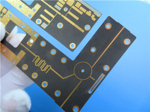
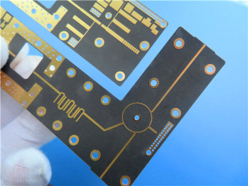
This is a custom 2-layer rigid PCB built on F4BTMS220 high-frequency substrate, specifically fabricated for microwave, RF, aerospace and radar-related circuit applications. With an ultra-thin finished thickness of 0.3mm, this board adopts a special bare copper design without solder mask and silkscreen on both sides, eliminating extra coating interference during high-frequency signal transmission. The board size is 36.4mm × 88.76mm with a dimensional tolerance of ±0.15mm. Manufactured strictly following IPC-Class-2 requirements and 100% electrically tested before shipment, this PCB delivers consistent and repeatable performance for high-end wireless and microwave system development worldwide.
PCB Specifications
This prototype PCB uses a pure through-hole design with no blind vias, simplifying signal paths and maintaining stable high-frequency transmission. It supports 6/7 mil minimum trace/space and 0.4mm minimum hole size, meeting standard precision requirements for RF circuit layout.
| Item |
Parameter |
| Base Material |
F4BTMS220 high-frequency PTFE ceramic laminate |
| Layer Count |
2-layer rigid |
| Board Dimension |
36.4mm × 88.76mm (±0.15mm) |
| Min Trace / Space |
6/7 mils |
| Min Hole Size |
0.4mm |
| Via Type |
Through-hole only |
| Board Thickness |
0.3mm |
| Copper Weight |
1oz outer layer copper |
| Via Plating |
20 μm |
| Surface Treatment |
Bare copper (no solder mask, no silkscreen, both sides) |
| Testing |
100% electrical test before delivery |
PCB Stack-up Structure
This 2-layer stack-up consists of double 35μm copper layers and a 0.254mm (10mil) F4BTMS220 core dielectric. This symmetric structure provides even mechanical balance and steady dielectric performance for high-frequency circuits.
| Layer |
Description |
| Top Copper |
35 μm copper layer |
| Dielectric Core |
F4BTMS220, 0.254mm (10mil) |
| Bottom Copper |
35 μm copper layer |
PCB Statistic
The design file is provided in standard Gerber RS-274-X format, fully compatible with professional PCB prototyping and mass production processes.
| Item |
Value |
| Components |
14 |
| Total Pads |
32 |
| Thru Hole Pads |
19 |
| Top SMT Pads |
13 |
| Bottom SMT Pads |
0 |
| Vias |
11 |
| Nets |
2 |

About F4BTMS220 Material
F4BTMS220 is an upgraded version of the conventional F4BTM series. Its formula blends ultra-fine glass fiber cloth and large amounts of uniformly distributed nano-ceramic fillers with PTFE resin. This material design greatly reduces the negative influence of glass fiber on electromagnetic wave propagation, effectively lowering dielectric loss and material anisotropy while improving dimensional stability and thermal conductivity.
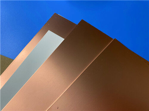
Compared with ordinary high-frequency substrates, F4BTMS220 features more stable dielectric temperature performance and lower thermal expansion coefficient. The material is equipped with low-roughness RTF copper foil as standard, which helps reduce conductor loss and maintain stable peel strength. It supports both copper and aluminum base bonding and is widely recognized as a reliable alternative to imported aerospace-grade high-frequency materials.
Product Features
Built with upgraded F4BTMS220 substrate, this PCB delivers genuine high-frequency advantages based on its inherent material characteristics:
Extremely low dielectric loss with Df as low as 0.0009 at 10GHz, supporting high-efficiency microwave signal transmission.
Fixed Dk 2.2 dielectric constant ensures consistent electrical performance across common RF frequency bands.
Low moisture absorption of 0.02% improves environmental adaptability for outdoor and aerospace applications.
Low-roughness RTF copper foil minimizes conductor loss and ensures stable circuit conductivity.
UL94-V0 flame retardant rating meets safety standards for aerospace and military-grade equipment.
Bare copper design removes solder mask interference, preserving the original high-frequency performance of the substrate.
Applications
This F4BTMS220 ultra-thin PCB is commonly used in high-reliability microwave and radio frequency systems that demand low loss and stable dielectric behavior:
- Aerospace and space cabin equipment
- Microwave and RF circuit modules
- Military radar systems
- Antenna feed networks
- Phase-sensitive antennas and phased array antennas
- Satellite communication devices
Conclusion
This custom 2-layer F4BTMS220 ultra-thin PCB provides stable low-loss performance for aerospace, radar and satellite communication projects. Adopting upgraded nano-ceramic filled PTFE material and RTF low roughness copper, the board maintains reliable electrical stability at high frequencies. All units pass complete electrical testing and comply with IPC-Class-2 standards. We support global shipping and welcome Gerber-based customization for prototype and small-batch production.


 Your message must be between 20-3,000 characters!
 English