logo
Products
PRODUCTS DETAILS
Home > Products >
10mil F4BTME350 Substrate 2-Layer Ultra-Thin Low Loss RF PCB

10mil F4BTME350 Substrate 2-Layer Ultra-Thin Low Loss RF PCB

MOQ: 1PCS
Price: USD9.99-99.99
Standard Packaging: Vacuum bags+Cartons
Delivery Period: 8-9 working days
Payment Method: T/T
Supply Capacity: 5000PCS per month
Detail Information
Place of Origin
CHINA
Brand Name
Bicheng
Certification
UL, ISO9001, IATF16949
Model Number
BIC-338.V1.0
Base Material:
F4BTME350
Layer Count:
2 Layers
PCB Thickness:
0.3mm Ultra-thin
PCB Size:
89.77mm × 45.16mm (±0.15mm Tolerance, 1PCS)
Solder Mask:
Black
Silkscreen:
White
Copper Weight:
1oz
Surface Finish:
Immersion Gold
Highlight:

Tin-plated Flexible Printed Circuit Board

,

Black Coating FPCB

,

Tin-plated FPCB

Product Description

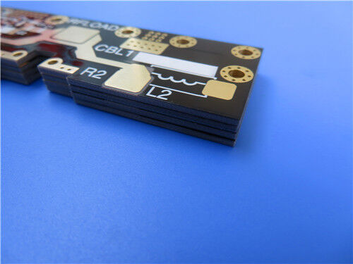
This custom F4BTME350 PCB is an ultra-thin high-frequency circuit board optimized for modern 4G/5G base station antennas, satellite communication, aerospace equipment, and multi-scenario RF/microwave modules. With an ultra-slim 0.3mm finished thickness and professional F4BTME350 nano-ceramic filled PTFE substrate, this board delivers stable low-loss signal performance and industry-grade ultra-low PIM (<-160 dBc) characteristics. Manufactured with precise 6/8 mil fine trace/space, 0.25mm micro-hole design, immersion gold surface finish, black top solder mask and white top silkscreen, the 89.77mm × 45.16mm PCB strictly follows IPC-Class-2 standards and undergoes 100% full electrical testing before shipment. It is a reliable high-frequency PCB solution for low-noise amplifiers, phased array antennas, automotive radar and high-power RF component projects worldwide.


PCB Specifications

This 2-layer F4BTME350 high-frequency PCB adopts a pure through-hole structure with no blind vias, ensuring clean and stable high-frequency signal transmission. All mechanical and electrical parameters are strictly calibrated for precision microwave circuit fabrication.

Specification Item Detailed Parameter
Base Material F4BTME350 nano-ceramic filled PTFE high-frequency laminate
Layer Configuration 2-layer rigid PCB
Board Dimensions 89.77mm × 45.16mm (±0.15mm tolerance, 1PCS)
Minimum Trace / Space 6/8 mils
Minimum Hole Size 0.25mm
Via Type Through-hole only, no blind vias
Finished Board Thickness 0.3mm ultra-thin
Outer Layer Copper Weight 1oz (1.4 mils) finished copper
Via Plating Thickness 20μm
Surface Finish Immersion Gold
Silkscreen Top: White; Bottom: None
Solder Mask Top: Black; Bottom: None
Pre-Shipment Test 100% full electrical testing


2-Layer PCB Stack-up Structure

The symmetrical ultra-thin stack-up features a 10mil F4BTME350 core dielectric layer, maintaining balanced mechanical stress and highly consistent dielectric performance for high-frequency microwave signal transmission.

Layer Structure Material & Thickness
Top Copper Layer 35μm conductive copper foil
Dielectric Core Substrate F4BTME350 Core, 0.254mm (10mil)
Bottom Copper Layer 35μm conductive copper foil


PCB Statistic

This prototype PCB is designed with compact circuit distribution, matching the layout requirements of miniaturized RF modules and antenna feed networks. Standard Gerber RS-274-X files support accurate prototyping and batch production.

Statistical Item Quantity / Format
Total Components 12
Total Pads 38
Thru Hole Pads 17
Top SMT Pads 21
Bottom SMT Pads 0
Vias 9
Nets 2


10mil F4BTME350 Substrate 2-Layer Ultra-Thin Low Loss RF PCB


F4BTME350 Material Overview

The F4BTME series laminates are manufactured through a meticulous process that involves the scientific formulation of glass fiber cloth, nano-ceramic fillers, and polytetrafluoroethylene (PTFE) resin. These substrates are built upon the F4BM dielectric layer and incorporate high dielectric constant and low loss nano-ceramics. This integration results in enhanced dielectric constant, superior heat resistance, reduced thermal expansion coefficient, increased insulation resistance, and improved thermal conductivity, all while maintaining low loss characteristics. Furthermore, F4BTME laminates are specifically paired with reverse-treated RTF copper foil, providing exceptional performance in terms of PIM, precise line control, and minimized conductor loss.


10mil F4BTME350 Substrate 2-Layer Ultra-Thin Low Loss RF PCB


F4BTME350 Material Features

Tailored for commercial and aerospace high-frequency scenarios, this F4BTME350 ultra-thin PCB solves common pain points of conventional RF boards:


Stable High-Frequency Performance: Fixed Dk 3.5 and low Df loss deliver consistent signal performance across 10GHz to 20GHz, avoiding frequency drift for 5G base station and satellite communication devices.


Ultra-Low PIM Stability: PIM lower than -160 dBc eliminates passive intermodulation interference, ensuring pure signal output for phased array antennas and low-noise amplifier modules.


Superior Thermal & Dimensional Stability: Ultra-low X/Y-axis CTE and low thermal Dk coefficient maintain stable electrical and mechanical performance under extreme temperature changes.


Low Conductor Loss & Fine Line Support: Matched with reverse-treated RTF copper foil, it supports precise line control and minimizes signal loss for high-power RF components.


High Environmental Adaptability: 0.05% ultra-low moisture absorption ensures reliable operation in outdoor base station, aerospace and vehicle radar environments.


Strict Deliver Quality: IPC-Class-2 manufacturing standard + 100% pre-shipment electrical test guarantees zero circuit defects and stable batch consistency.


Applications

F4BTME350 2-layer ultra-thin PCBs are widely adopted in high-precision, low-interference RF and microwave systems:


  • 4G/5G base station antennas and PCS/PCN large-format antenna feed networks
  • Low Noise Amplifiers (LNAs), LNBs/LNCs and high-power RF amplifiers
  • Phased array antennas and phase-sensitive antenna systems
  • Satellite communication terminals, aerospace and cabin equipment
  • Microwave RF modules, automotive radar and military radar systems
  • RF passive components: power dividers, couplers and combiners


Conclusion

This custom F4BTME350 2-layer ultra-thin rigid PCB provides cost-effective, high-stability solutions for commercial 5G communication, satellite and aerospace RF projects. Built with genuine F4BTME350 nano-ceramic PTFE substrate and RTF copper foil, it features low signal loss, ultra-low PIM and excellent thermal stability. All boards are fully electrically tested and compliant with IPC-Class-2 standards. We support global shipping and flexible customization for RF prototype verification and mass production orders.


10mil F4BTME350 Substrate 2-Layer Ultra-Thin Low Loss RF PCB

Products
PRODUCTS DETAILS
10mil F4BTME350 Substrate 2-Layer Ultra-Thin Low Loss RF PCB
MOQ: 1PCS
Price: USD9.99-99.99
Standard Packaging: Vacuum bags+Cartons
Delivery Period: 8-9 working days
Payment Method: T/T
Supply Capacity: 5000PCS per month
Detail Information
Place of Origin
CHINA
Brand Name
Bicheng
Certification
UL, ISO9001, IATF16949
Model Number
BIC-338.V1.0
Base Material:
F4BTME350
Layer Count:
2 Layers
PCB Thickness:
0.3mm Ultra-thin
PCB Size:
89.77mm × 45.16mm (±0.15mm Tolerance, 1PCS)
Solder Mask:
Black
Silkscreen:
White
Copper Weight:
1oz
Surface Finish:
Immersion Gold
Minimum Order Quantity:
1PCS
Price:
USD9.99-99.99
Packaging Details:
Vacuum bags+Cartons
Delivery Time:
8-9 working days
Payment Terms:
T/T
Supply Ability:
5000PCS per month
Highlight

Tin-plated Flexible Printed Circuit Board

,

Black Coating FPCB

,

Tin-plated FPCB

Product Description

This custom F4BTME350 PCB is an ultra-thin high-frequency circuit board optimized for modern 4G/5G base station antennas, satellite communication, aerospace equipment, and multi-scenario RF/microwave modules. With an ultra-slim 0.3mm finished thickness and professional F4BTME350 nano-ceramic filled PTFE substrate, this board delivers stable low-loss signal performance and industry-grade ultra-low PIM (<-160 dBc) characteristics. Manufactured with precise 6/8 mil fine trace/space, 0.25mm micro-hole design, immersion gold surface finish, black top solder mask and white top silkscreen, the 89.77mm × 45.16mm PCB strictly follows IPC-Class-2 standards and undergoes 100% full electrical testing before shipment. It is a reliable high-frequency PCB solution for low-noise amplifiers, phased array antennas, automotive radar and high-power RF component projects worldwide.


PCB Specifications

This 2-layer F4BTME350 high-frequency PCB adopts a pure through-hole structure with no blind vias, ensuring clean and stable high-frequency signal transmission. All mechanical and electrical parameters are strictly calibrated for precision microwave circuit fabrication.

Specification Item Detailed Parameter
Base Material F4BTME350 nano-ceramic filled PTFE high-frequency laminate
Layer Configuration 2-layer rigid PCB
Board Dimensions 89.77mm × 45.16mm (±0.15mm tolerance, 1PCS)
Minimum Trace / Space 6/8 mils
Minimum Hole Size 0.25mm
Via Type Through-hole only, no blind vias
Finished Board Thickness 0.3mm ultra-thin
Outer Layer Copper Weight 1oz (1.4 mils) finished copper
Via Plating Thickness 20μm
Surface Finish Immersion Gold
Silkscreen Top: White; Bottom: None
Solder Mask Top: Black; Bottom: None
Pre-Shipment Test 100% full electrical testing


2-Layer PCB Stack-up Structure

The symmetrical ultra-thin stack-up features a 10mil F4BTME350 core dielectric layer, maintaining balanced mechanical stress and highly consistent dielectric performance for high-frequency microwave signal transmission.

Layer Structure Material & Thickness
Top Copper Layer 35μm conductive copper foil
Dielectric Core Substrate F4BTME350 Core, 0.254mm (10mil)
Bottom Copper Layer 35μm conductive copper foil


PCB Statistic

This prototype PCB is designed with compact circuit distribution, matching the layout requirements of miniaturized RF modules and antenna feed networks. Standard Gerber RS-274-X files support accurate prototyping and batch production.

Statistical Item Quantity / Format
Total Components 12
Total Pads 38
Thru Hole Pads 17
Top SMT Pads 21
Bottom SMT Pads 0
Vias 9
Nets 2


10mil F4BTME350 Substrate 2-Layer Ultra-Thin Low Loss RF PCB


F4BTME350 Material Overview

The F4BTME series laminates are manufactured through a meticulous process that involves the scientific formulation of glass fiber cloth, nano-ceramic fillers, and polytetrafluoroethylene (PTFE) resin. These substrates are built upon the F4BM dielectric layer and incorporate high dielectric constant and low loss nano-ceramics. This integration results in enhanced dielectric constant, superior heat resistance, reduced thermal expansion coefficient, increased insulation resistance, and improved thermal conductivity, all while maintaining low loss characteristics. Furthermore, F4BTME laminates are specifically paired with reverse-treated RTF copper foil, providing exceptional performance in terms of PIM, precise line control, and minimized conductor loss.


10mil F4BTME350 Substrate 2-Layer Ultra-Thin Low Loss RF PCB


F4BTME350 Material Features

Tailored for commercial and aerospace high-frequency scenarios, this F4BTME350 ultra-thin PCB solves common pain points of conventional RF boards:


Stable High-Frequency Performance: Fixed Dk 3.5 and low Df loss deliver consistent signal performance across 10GHz to 20GHz, avoiding frequency drift for 5G base station and satellite communication devices.


Ultra-Low PIM Stability: PIM lower than -160 dBc eliminates passive intermodulation interference, ensuring pure signal output for phased array antennas and low-noise amplifier modules.


Superior Thermal & Dimensional Stability: Ultra-low X/Y-axis CTE and low thermal Dk coefficient maintain stable electrical and mechanical performance under extreme temperature changes.


Low Conductor Loss & Fine Line Support: Matched with reverse-treated RTF copper foil, it supports precise line control and minimizes signal loss for high-power RF components.


High Environmental Adaptability: 0.05% ultra-low moisture absorption ensures reliable operation in outdoor base station, aerospace and vehicle radar environments.


Strict Deliver Quality: IPC-Class-2 manufacturing standard + 100% pre-shipment electrical test guarantees zero circuit defects and stable batch consistency.


Applications

F4BTME350 2-layer ultra-thin PCBs are widely adopted in high-precision, low-interference RF and microwave systems:


  • 4G/5G base station antennas and PCS/PCN large-format antenna feed networks
  • Low Noise Amplifiers (LNAs), LNBs/LNCs and high-power RF amplifiers
  • Phased array antennas and phase-sensitive antenna systems
  • Satellite communication terminals, aerospace and cabin equipment
  • Microwave RF modules, automotive radar and military radar systems
  • RF passive components: power dividers, couplers and combiners


Conclusion

This custom F4BTME350 2-layer ultra-thin rigid PCB provides cost-effective, high-stability solutions for commercial 5G communication, satellite and aerospace RF projects. Built with genuine F4BTME350 nano-ceramic PTFE substrate and RTF copper foil, it features low signal loss, ultra-low PIM and excellent thermal stability. All boards are fully electrically tested and compliant with IPC-Class-2 standards. We support global shipping and flexible customization for RF prototype verification and mass production orders.


10mil F4BTME350 Substrate 2-Layer Ultra-Thin Low Loss RF PCB