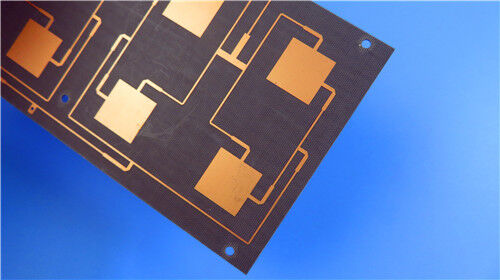
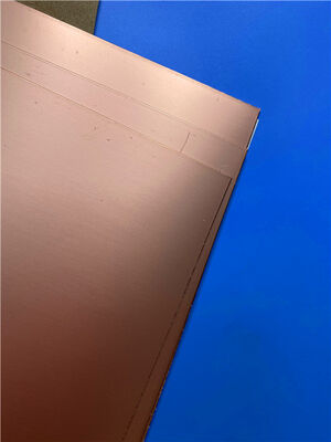
This 2-layer rigid F4BME220 PCB is an ultra-thin, cost-optimized high-frequency solution designed for commercial radio frequency circuitry and wireless signal processing devices. Utilizing upgraded F4BME-series fiberglass-reinforced PTFE composite dielectric, this PCB delivers enhanced electrical stability and superior signal transmission consistency compared with conventional F4B substrate boards. Boasting an ultra-slim 0.1mm finished thickness and 1 oz outer-layer copper weighting, the board adopts immersion gold surface finishing to sustain durable conductivity and anti-oxidation performance. It supports precision 5/8 mil line/space fabrication and 0.25mm micro-hole machining with a non-blind-via structural design. The board features top-side white silkscreen and green solder mask, while the bottom side remains fully uncoated.
PCB Specification
| Specification Item |
Details |
| Base Material |
F4BME220 fiberglass-reinforced PTFE composite substrate |
| Layer Count |
2 layers (rigid PCB) |
| Finished Board Thickness |
0.1mm |
| Board Dimensions |
79mm x 65.3mm (1PCS), tolerance +/-0.15mm |
| Finished Copper Weight |
1 oz (1.4 mils) outer layers |
| Via Plating Thickness |
20 μm |
| Minimum Trace/Space |
5/8 mils |
| Minimum Hole Size |
0.25mm |
| Blind Vias |
None |
| Surface Finish |
Immersion Gold |
| Silkscreen |
White top silkscreen, no bottom silkscreen |
| Solder Mask |
Green top solder mask, no bottom solder mask |
| Quality Standard |
IPC-Class-2 |
| Testing Process |
100% electrical test prior to shipment |
PCB Stack-up Structure
Adopting a symmetrical dual-layer rigid layout with an ultra-thin dielectric core, this stackup structure ensures exceptional mechanical flatness and uniform electrical characteristics. The balanced layer configuration delivers consistent high-frequency signal transmission performance and stable manufacturing repeatability, perfectly matching the design demands of compact commercial RF circuit modules.
| Stack-up Layer |
Specification Details |
| Copper Layer 1 |
35 μm RTF copper foil |
| F4BME220 Substrate Core |
0.1mm fiberglass & PTFE composite dielectric core |
| Copper Layer 2 |
35 μm RTF copper foil |

PCB Statistic
This ultra-thin F4BME220 high-frequency PCB features refined component arrangement and rational via layout, catering to miniaturized assembly requirements and delivering steady electrical signal output for compact commercial RF functional modules.
| Statistical Item |
Quantity |
| Total Components |
23 |
| Total Pads |
26 |
| Thru Hole Pads |
14 |
| Top SMT Pads |
12 |
| Bottom SMT Pads |
0 |
| Vias Quantity |
37 |
| Nets Quantity |
2 |
F4BME High-Frequency Substrate Introduction
F4BME-series laminates are premium composite dielectric materials, fabricated through precise material proportioning and high-standard lamination of fiberglass cloth, PTFE resin and PTFE film layers. Compared with traditional F4B substrates, this upgraded material series offers a broader adjustable dielectric constant range, lower signal attenuation, higher insulation resistance and more stable electrical performance. It serves as a high-reliability alternative to imported equivalent high-frequency dielectric materials for commercial RF PCB manufacturing.
F4BME Series Core Characteristics
Tailored with customized dielectric formulations and mature manufacturing techniques, F4BME composite laminates deliver comprehensive high-frequency performance and outstanding cost efficiency, fully adaptable to large-scale commercial production scenarios:
Fully customizable dielectric constant, with optional DK values ranging from 2.17 to 3.0 to accommodate diverse circuit design specifications
Low dielectric loss property minimizes signal energy attenuation during high-frequency signal transmission
Comes standard with RTF copper foil, providing superior PIM performance for high-sensitivity radio frequency application scenarios
Supports diversified dimensional customization, enabling flexible size adjustment and effective overall cost control
Features excellent irradiation resistance and low outgassing properties, ensuring stable operation in complex and harsh working environments
Boasts high commercial maturity and mass production compatibility, delivering remarkable cost performance for batch manufacturing
Typical Applications
Benefiting from tunable dielectric parameters, low-loss transmission characteristics and high cost-effectiveness, F4BME220 PCBs are widely deployed in commercial high-frequency radio frequency hardware and wireless communication infrastructure systems:
- Commercial radio frequency signal processing and radar detection systems
- High-frequency phase tuning modules and RF passive electronic components
- RF power distribution, signal coupling and signal synthesis units
- Antenna signal feed systems and phased array antenna arrays
- Satellite communication terminal devices and commercial cellular base station antennas
Quality & Service Guarantee
All F4BME220 ultra-thin high-frequency PCBs are fabricated in full adherence to IPC-Class-2 industrial quality specifications. Manufactured based on standard Gerber RS-274-X data, these circuit boards maintain rigorous dimensional accuracy and consistent electrical reproducibility, complying with formal batch-production criteria for high-frequency commercial applications. Each finished unit undergoes complete electrical performance verification prior to shipment to ensure zero functional defects and stable batch-to-batch consistency. With global supply capabilities and standardized technical support, these low-loss PCB solutions deliver dependable, repeatable performance for commercial RF fabrication and wireless communication infrastructure projects across global markets.


 Your message must be between 20-3,000 characters!
 English