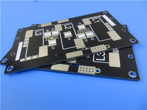
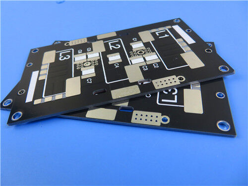
This 2-layer F4BTMS450 rigid PCB is a high-reliability, low-loss high-frequency circuit solution engineered for aerospace-grade equipment, military radar systems, and precision RF microwave applications. Utilizing the upgraded F4BTMS450 ceramic-filled PTFE substrate paired with premium low-roughness RTF copper foil, this rigid circuit board features a 0.6mm finished thickness and eco-friendly lead-free HASL surface finish. Every unit undergoes strict 100% electrical testing prior to delivery and complies fully with IPC-Class-2 industrial reliability criteria. Featuring ultra-stable dielectric properties, minimized multi-axis anisotropy, and superior thermo-mechanical robustness, this PCB delivers consistent performance for high-end aerospace devices, phased array antenna systems, and satellite communication terminals. We welcome global customers to submit Gerber RS-274-X files for custom quotations, with worldwide shipping and full professional technical support available.
What Is F4BTMS450? Advanced Substrate Introduction
F4BTMS450 serves as an enhanced high-performance iteration of the conventional F4BTM material series, refined through optimized material formulations and advanced manufacturing processes. Incorporated with high-content nano-ceramic fillers and reinforced by ultra-thin, ultra-fine woven fiberglass, this upgraded substrate achieves comprehensive performance improvements and highly stable dielectric parameters. It acts as a reliable alternative to imported equivalent high-frequency materials, perfectly catering to high-standard industrial and aerospace electronic applications.
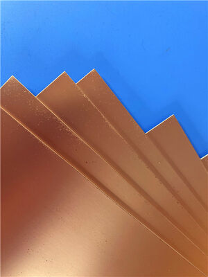
The substrate adopts a sophisticated composite structure composed of PTFE resin, uniformly dispersed specialized nano-ceramic particles, and minimal ultra-thin fiberglass reinforcement. This innovative design effectively mitigates the adverse effects of fiberglass on electromagnetic wave propagation, significantly reducing dielectric loss and X/Y/Z-axis material anisotropy. It delivers exceptional dimensional stability, expanded effective frequency bandwidth, enhanced electrical strength, and improved thermal conductivity, alongside ultra-low thermal expansion coefficients and temperature-insensitive dielectric characteristics. The standardized low-roughness RTF copper foil further lowers high-frequency conductor loss while maintaining excellent copper peel strength, supporting both copper-based and aluminum-based PCB structural designs.

Key Features of F4BTMS450 PCB
Integrating outstanding electrical stability, reliable thermal performance, and robust mechanical durability, the F4BTMS450 substrate fully satisfies the rigorous operating standards of aerospace and military high-frequency circuit systems:
Stable Dielectric Constant (Dk): Maintains a precise dielectric constant of 4.5 ±0.09 at 10GHz, enabling accurate impedance matching and reliable high-frequency signal transmission
Ultra-Low Dissipation Factor (Df): Boasts ultra-low loss tangents of 0.0015 at 10GHz and 0.0019 at 20GHz, effectively suppressing high-frequency signal attenuation and power loss
Excellent Thermal Dimensional Stability: Features low linear CTE values of 12 ppm/°C for both X and Y axes, and 45 ppm/°C for the Z axis across -55°C to 288°C, preventing board warpage and circuit failure under extreme temperature cycling
Minimal Dielectric Temperature Drift: Offers an ultra-low thermal coefficient of Dk (-58 ppm/°C) within -55°C to 150°C, ensuring consistent electrical performance in dynamically changing thermal environments
Superior Thermal Conductivity: With a thermal conductivity of 0.64 W/MK, it accelerates heat dissipation and enhances the long-term operational stability of high-power RF circuits
Low Moisture Sensitivity: Achieves an ultra-low moisture absorption rate of 0.08%, preventing electrical parameter deviations induced by humid working conditions
High Flame Retardancy: Meets UL-94 V0 flame retardant standards, guaranteeing safe and stable operation for aerospace and military electronic systems
Key PCB Construction Specifications
| Parameter Item |
Specific Specification |
| Base Material |
F4BTMS450 high-reliability ceramic-filled PTFE substrate |
| Layer Count |
2 layers (rigid structure) |
| Board Dimensions |
38.4mm × 56.35mm (±0.15mm tolerance, 1 piece) |
| Minimum Trace/Space |
4/6 mils, supporting ultra-fine trace fabrication |
| Minimum Hole Size |
0.3mm |
| Via Design |
No blind or buried vias |
| Finished Board Thickness |
0.6mm |
| Finished Copper Weight |
1oz (1.4 mils) outer copper layers adopting low-roughness RTF foil |
| Via Plating Thickness |
20μm |
| Surface Finish |
Lead-Free HASL |
| Silkscreen |
White top silkscreen with no bottom silkscreen |
| Solder Mask |
Black top solder mask, no bottom solder mask |
| Quality Test Standard |
100% full-scale electrical testing implemented before shipment |
2-Layer F4BTMS450 PCB Stack-up Structure
This standardized 2-layer rigid stack-up utilizes premium F4BTMS450 ceramic-filled dielectric core material. It features ultra-low multi-axis anisotropy and evenly distributed structural stress, perfectly matching the high-stability performance demands of aerospace RF and microwave circuit applications:
| Layer Sequence |
Material Specification |
Thickness |
Core Function |
| Outer Layer 1 (Top) |
Low roughness RTF conductive copper foil |
35μm |
Serves as the primary platform for high-frequency RF signal transmission and surface-mount component soldering |
| Core Dielectric Layer |
F4BTMS450 high-reliability ceramic composite core substrate |
0.508mm (20mil) |
Provides low-loss dielectric isolation, minimal structural anisotropy, and stable temperature-resistant dielectric performance for high-frequency circuits |
| Outer Layer 2 (Bottom) |
Low roughness RTF conductive copper foil |
35μm |
Supplementary circuit transmission layer that balances overall structural stability of the PCB |
PCB Statistics
| Parameter Item |
Specific Value |
| Components |
13 |
| Total Pads |
20 |
| Thru Hole Pads |
12 |
| Top SMT Pads |
8 |
| Bottom SMT Pads |
0 |
| Vias |
9 |
| Nets |
5 |
Accepted Artwork Format: We accept standard Gerber RS-274-X design files from global clients. This universal industry-standard format supports precise technical evaluation, customized price quoting, and streamlined mass production.
Production Quality Standard: All PCBs are manufactured and inspected in strict compliance with IPC-Class-2 industrial reliability specifications.
Global Supply Service: We offer worldwide customized PCB quotation and international shipping solutions. Global customers can submit Gerber files for exclusive custom quotes.
Typical Application Scenarios
- Aerospace equipment, space and cabin equipment
- Microwave, RF
- Radar, military radar
- Feed networks
- Phase-sensitive antennas, phased array antennas
- Satellite communications, and more


 Your message must be between 20-3,000 characters!
 English