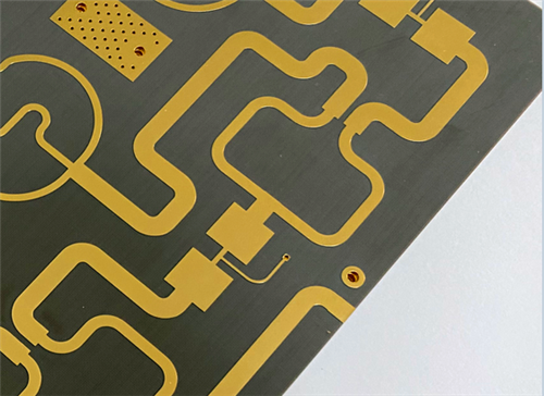
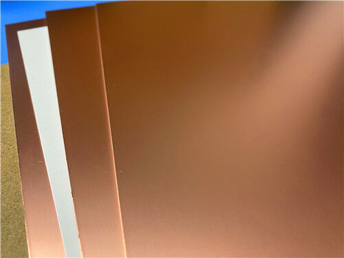
This 2-layer TLY-5 rigid PCB is a premium ultra-low-loss high-frequency circuit board tailored for millimeter-wave and high-precision RF applications. Built with high-stability TLY-5 woven fiberglass-reinforced PTFE laminate, this rigid PCB features a 0.3mm finished board thickness and reliable EPIG surface finish, paired with 1oz outer-layer copper. Produced under strict IPC-Class-2 guidelines and 100% electrically tested prior to delivery, it delivers minimal dielectric loss, outstanding dimensional stability, and steady electrical performance for 77GHz automotive radar, satellite communication, Ka/E/W-band millimeter-wave equipment, and aerospace high-reliability systems. We welcome global Gerber file inquiries and offer worldwide shipping.
What Is TLY-5 Laminate? High-Stability Low-Loss Substrate Introduction
TLY-5 represents a premium grade of high-frequency PTFE composite substrate, utilizing ultra-light woven fiberglass reinforcement to achieve far better dimensional stability than conventional chopped-fiber PTFE materials. Its refined woven structural matrix enhances overall mechanical uniformity and structural consistency, making TLY-5 an ideal choice for large-scale mass production.
Thanks to its ultra-low dissipation factor and tightly controlled dielectric constant tolerance, TLY-5 substrates sustain stable signal transmission across diverse millimeter-wave frequency bands. It effectively mitigates high-frequency signal attenuation, frequency drift, and structural deformation issues commonly found in ordinary high-frequency PCBs, ensuring long-term dependable operation for precision radar, wireless communication, and RF amplifier systems.

Core Performance Features of TLY-5 High-Frequency PCB
The TLY-5 substrate delivers superior electrical, physical, and thermal characteristics, fully satisfying rigorous industrial and aerospace-grade standards for high-frequency circuit operation:
Precise Dielectric Constant (Dk): Stable Dk of 2.2 with a tight tolerance of ±0.02 at 10 GHz/23°C, ensuring consistent high-frequency signal transmission accuracy
Ultra-Low Dissipation Factor (Df): Extremely low loss tangent of 0.0009 at 10GHz, minimizing high-frequency signal attenuation and transmission loss
Stable Physical Density: Standard specific gravity of 2.19 g/cm3, realizing lightweight PCB design while maintaining structural rigidity
Superior Moisture Resistance: Ultra-low moisture absorption rate of 0.02%, preventing electrical performance degradation in humid working environments
Controllable Thermal Expansion Coefficient (CTE): X-axis 26 ppm/°C, Y-axis 15 ppm/°C, Z-axis 217 ppm/°C, matching copper foil expansion and contraction to avoid board cracking and circuit failure
Key Benefits of TLY-5 PCB
Featuring balanced and comprehensive performance strengths, TLY-5 woven fiberglass PTFE substrates outperform many mainstream high-frequency materials, providing stable, cost-effective, and high-reliability solutions for advanced RF and millimeter-wave applications:
Excellent Dimensional Stability: Woven fiberglass structure avoids deformation and size deviation during processing and long-term use
Industry-Leading Low DF Performance: Ultra-low loss tangent ensures ultra-low attenuation transmission for millimeter wave signals
Superior Moisture Resistance: Low moisture absorption adapts to complex environmental working conditions
High Copper Peel Strength: Reliable bonding performance between copper foil and substrate, avoiding circuit peeling and failure
Uniform and Consistent DK: Tight dielectric constant tolerance ensures batch product performance consistency
Key PCB Construction Specifications
| Parameter Item |
Specific Specification |
| Base Material |
TLY-5 woven fiberglass reinforced PTFE laminate |
| Layer Count |
2 layers (rigid structure) |
| Board Dimensions |
45mm × 87mm (±0.15mm tolerance, 1 piece) |
| Minimum Trace/Space |
6/10 mils, adapting to high-precision RF circuit design |
| Minimum Hole Size |
0.4mm |
| Via Design |
No blind vias, only through-hole vias for stable structure |
| Finished Board Thickness |
0.3mm, ultra-thin for compact millimeter wave device integration |
| Finished Copper Weight |
1oz (1.4 mils) outer copper layers, stable current carrying and signal transmission |
| Via Plating Thickness |
20μm, ensuring reliable via conductivity and oxidation resistance |
| Surface Finish |
EPIG, optimizing soldering reliability and component adhesion |
| Silkscreen |
No top & bottom silkscreen, ensuring pure high-frequency signal transmission |
| Solder Mask |
No top & bottom solder mask |
| Quality Test Standard |
100% full electrical testing before shipment to eliminate open/short circuit defects |
2-Layer TLY-5 PCB Stack-up Structure
This standardized 2-layer rigid stack-up adopts high-stability TLY-5 dielectric material, featuring balanced layered stress distribution and exceptional high-frequency signal stability, perfectly suited for professional millimeter-wave operating environments:
| Layer Sequence |
Material Specification |
Thickness |
Core Function |
| Outer Layer 1 (Top) |
Conductive Copper Foil |
35μm |
Millimeter wave signal transmission and component soldering carrier |
| Core Dielectric Layer |
TLY-5 high-frequency PTFE laminate |
0.191mm (7.5mil) |
Low-loss dielectric isolation, stable high-frequency signal transmission foundation |
| Outer Layer 2 (Bottom) |
Conductive Copper Foil |
35μm |
Auxiliary circuit transmission and structural balance support |
PCB Statistics
| Parameter Item |
Specific Value |
| Components |
37 |
| Total Pads |
149 |
| Thru Hole Pads |
85 |
| Top SMT Pads |
64 |
| Bottom SMT Pads |
0 |
| Vias |
139 |
| Nets |
2 |
Accepted Artwork Format: We accept standard Gerber files RS-274-X format from global clients. This industry-standard file format enables precise technical evaluation, accurate custom quoting, and streamlined formal production, ensuring smooth, error-free technical collaboration for all international PCB customization projects.
Production Quality Standard: All TLY-5 high-frequency PCBs are manufactured and inspected in strict accordance with IPC-Class-2 industrial reliability specifications. Rigorous standardized production and quality control procedures guarantee consistent dimensional precision and stable electrical performance for every production batch.
Global Supply Service: We provide worldwide customized PCB quotation and international shipping services. Clients globally can submit Gerber files for exclusive custom quotes, and we deliver full one-stop solutions covering PCB quotation, precision manufacturing, comprehensive quality inspection, and global logistics delivery.
Typical Application Scenarios
Combining ultra-low signal loss, outstanding structural stability, and superior millimeter-wave frequency performance, TLY-5 2-layer PCBs are widely adopted in high-end RF systems, millimeter-wave devices, and aerospace precision electronic equipment:
Automotive Radar: 77GHz vehicle-mounted millimeter wave radar detection systems
Satellite & Cellular Communications: Satellite communication terminals and cellular base station RF modules
Power Amplifiers: High-frequency RF power amplifier circuit boards
LNB, LNA & LNC Devices: Low-noise amplifiers and low-noise block downconverters
Aerospace Equipment: Aerospace precision communication and detection modules
Millimeter Wave Band Applications: Professional Ka-band, E-band, and W-band high-frequency devices


 Your message must be between 20-3,000 characters!
 English