logo
Products
PRODUCTS DETAILS
Home > Products >
High DK PCB TP1020 Double-Sided 1.6mm Pure Gold Circuit Board

High DK PCB TP1020 Double-Sided 1.6mm Pure Gold Circuit Board

MOQ: 1PCS
Price: USD9.99-99.99
Standard Packaging: Vacuum bags+Cartons
Delivery Period: 8-9 working days
Payment Method: T/T
Supply Capacity: 5000PCS per month
Detail Information
Place of Origin
CHINA
Brand Name
Bicheng
Certification
UL, ISO9001, IATF16949
Model Number
BIC-312.V1.0
Base Material:
TP1020
Layer Count:
2 Layers
PCB Thickness:
1.6 Mm
PCB Size:
55.53 Mm × 104 Mm Per Piece, Tolerance ±0.15 Mm
Solder Mask:
No
Silkscreen:
No
Copper Weight:
1oz (1.4 Mils) Outer Layers
Surface Finish:
Pure Gold
Highlight:

High DK PCB TP1020

,

Double-Sided 1.6mm PCB

,

Pure Gold RF PCB Board

Product Description

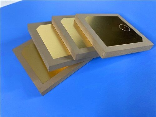
This double-sided high-frequency PCB uses TP1020 as its core dielectric and carries pure gold plating. No silkscreen is printed on either side, and neither surface receives solder mask. This board fits compact radio-frequency circuits that demand stable high-Dk performance and dependable signal consistency, especially for hardware built around small antennas and navigation systems.


PCB Specifications

Item Details
Base material TP1020
Layer count Double sided
Board dimensions 55.53 mm × 104 mm per piece, tolerance ±0.15 mm
Minimum Trace / Space 4 / 6 mils
Minimum Hole Size 0.5 mm
Blind vias None
Finished board thickness 1.6 mm
Finished copper weight 1 oz (1.4 mils) outer layers
Via plating thickness 20 μm
Surface finish Pure Gold
Top Silkscreen No
Bottom Silkscreen No
Top Solder Mask No
Bottom Solder Mask No
Pre-shipment check 100% electrical test


Gerber RS-274-X is the accepted artwork format. All fabrication follows IPC-Class-2, and these circuit boards can be shipped to customers worldwide.


PCB Stack-up

This two-layer rigid stack consists of a single TP1020 core sandwiched between two copper foils.

Layer Material & Thickness
Copper_layer_1 35 μm
TP1020 Core 1.5 mm (59 mil)
Copper_layer_2 35 μm


PCB Statistics

Item Quantity
Components 64
Total Pads 130
Thru Hole Pads 81
Top SMT Pads 49
Bottom SMT Pads 0
Vias 84
Nets 2


High DK PCB TP1020 Double-Sided 1.6mm Pure Gold Circuit Board


About TP Series Laminates

TP material stands out as a distinctive high-frequency thermoplastic option. Its dielectric layer combines ceramic filler and polyphenylene oxide resin, with no fiberglass reinforcement. Tuning the ratio between ceramic and PPO resin allows precise adjustment of dielectric constant. It relies on a specialised manufacturing route and delivers consistent dielectric behaviour together with high reliability. TP denotes unclad smooth substrate; TP-1 carries copper on one face, while TP-2 is copper-clad on both sides.


The dielectric constant can be selected freely from 3 to 25 to match circuit requirements and remains stable across operating conditions. Popular grades include 3.0, 4.4, 6.0, 6.15, 9.2, 9.6, 9.8, 10.2, 11, 16 and 20. Dielectric loss stays low. Loss rises as frequency climbs, yet the shift remains modest below 10 GHz. Corresponding part numbers cover TP300, TP440, TP600, TP615, TP920, TP960, TP980, TP1020 and others.


This family also features strong resistance to radiation and low outgassing. Bond strength between copper foil and dielectric surpasses vacuum-deposited metal on ceramic substrates. The substrate lends itself well to machining, including drilling, turning, grinding, shearing and etching, operations difficult to carry out on bare ceramic. Fabrication runs with good yields and costs less than equivalent ceramic substrates. It is generally not recommended for multilayer builds; if multilayers are required, low-temperature prepreg should be selected and feasibility carefully assessed. The material cannot withstand thermal shock at 260 °C and is not suitable for wave soldering. Hand soldering with a constant-temperature iron is preferred. Reflow work, if attempted, should not exceed 200 °C, with full review of stability risks. Its continuous operating window runs from −100 °C to +150 °C; exposure above 180 °C may trigger deformation, copper delamination and noticeable drift in electrical properties. Minimum available thickness starts at 0.5 mm, with a broad range of custom thickness options.


High DK PCB TP1020 Double-Sided 1.6mm Pure Gold Circuit Board


Applications

  • Global Satellite Navigation System
  • Missile-borne systems
  • Fuze technology
  • Miniaturized antennas


Typical Value of TP1020
Product Technical Parameter   Value
Product Features Test Conditions Unit TP1020
Dielectric Constant 10GHz. / 10.2±0.2
Dielectric Constant Tolerance / / ±2%
Loss Tangent 10GHz / 0.0012
Dielectric Constant Temperature Coefficient -55 º~150ºC PPM/℃ -40
Peel Strength 1 OZ Normal State N/mm >0.6
1 OZ After AC Humidity Test N/mm >0.4
Volume Resistivity Normal State at 500V MΩ.cm >1×10⁹
Surface Resistivity Normal State at 500V MΩ >1×10⁷
Coefficient of Thermal Expansion
(XY Z)
-55 º~150ºC PPM/℃ 40,40,55
Water Absorption 20±2℃, 24 hours % ≤0.01
Long-Term Operating Temperature High-Low Temperature Chamber ℃ -100º~150ºC
Density / g/cm3 2.33
Thermal Conductivity / W/MK 0.67
Material Composition PPE, ceramic, paired with ED copper foil.


This TP1020 circuit board is a practical choice for projects calling for high, stable dielectric constant and low loss at microwave frequencies. Fabrication complies with IPC-Class-2, and orders for small prototype batches as well as larger production runs can be shipped globally. Submit Gerber files to receive pricing details. You may reach out anytime to ask about lead times for these high-frequency thermoplastic PCB.


High DK PCB TP1020 Double-Sided 1.6mm Pure Gold Circuit Board

Products
PRODUCTS DETAILS
High DK PCB TP1020 Double-Sided 1.6mm Pure Gold Circuit Board
MOQ: 1PCS
Price: USD9.99-99.99
Standard Packaging: Vacuum bags+Cartons
Delivery Period: 8-9 working days
Payment Method: T/T
Supply Capacity: 5000PCS per month
Detail Information
Place of Origin
CHINA
Brand Name
Bicheng
Certification
UL, ISO9001, IATF16949
Model Number
BIC-312.V1.0
Base Material:
TP1020
Layer Count:
2 Layers
PCB Thickness:
1.6 Mm
PCB Size:
55.53 Mm × 104 Mm Per Piece, Tolerance ±0.15 Mm
Solder Mask:
No
Silkscreen:
No
Copper Weight:
1oz (1.4 Mils) Outer Layers
Surface Finish:
Pure Gold
Minimum Order Quantity:
1PCS
Price:
USD9.99-99.99
Packaging Details:
Vacuum bags+Cartons
Delivery Time:
8-9 working days
Payment Terms:
T/T
Supply Ability:
5000PCS per month
Highlight

High DK PCB TP1020

,

Double-Sided 1.6mm PCB

,

Pure Gold RF PCB Board

Product Description

This double-sided high-frequency PCB uses TP1020 as its core dielectric and carries pure gold plating. No silkscreen is printed on either side, and neither surface receives solder mask. This board fits compact radio-frequency circuits that demand stable high-Dk performance and dependable signal consistency, especially for hardware built around small antennas and navigation systems.


PCB Specifications

Item Details
Base material TP1020
Layer count Double sided
Board dimensions 55.53 mm × 104 mm per piece, tolerance ±0.15 mm
Minimum Trace / Space 4 / 6 mils
Minimum Hole Size 0.5 mm
Blind vias None
Finished board thickness 1.6 mm
Finished copper weight 1 oz (1.4 mils) outer layers
Via plating thickness 20 μm
Surface finish Pure Gold
Top Silkscreen No
Bottom Silkscreen No
Top Solder Mask No
Bottom Solder Mask No
Pre-shipment check 100% electrical test


Gerber RS-274-X is the accepted artwork format. All fabrication follows IPC-Class-2, and these circuit boards can be shipped to customers worldwide.


PCB Stack-up

This two-layer rigid stack consists of a single TP1020 core sandwiched between two copper foils.

Layer Material & Thickness
Copper_layer_1 35 μm
TP1020 Core 1.5 mm (59 mil)
Copper_layer_2 35 μm


PCB Statistics

Item Quantity
Components 64
Total Pads 130
Thru Hole Pads 81
Top SMT Pads 49
Bottom SMT Pads 0
Vias 84
Nets 2


High DK PCB TP1020 Double-Sided 1.6mm Pure Gold Circuit Board


About TP Series Laminates

TP material stands out as a distinctive high-frequency thermoplastic option. Its dielectric layer combines ceramic filler and polyphenylene oxide resin, with no fiberglass reinforcement. Tuning the ratio between ceramic and PPO resin allows precise adjustment of dielectric constant. It relies on a specialised manufacturing route and delivers consistent dielectric behaviour together with high reliability. TP denotes unclad smooth substrate; TP-1 carries copper on one face, while TP-2 is copper-clad on both sides.


The dielectric constant can be selected freely from 3 to 25 to match circuit requirements and remains stable across operating conditions. Popular grades include 3.0, 4.4, 6.0, 6.15, 9.2, 9.6, 9.8, 10.2, 11, 16 and 20. Dielectric loss stays low. Loss rises as frequency climbs, yet the shift remains modest below 10 GHz. Corresponding part numbers cover TP300, TP440, TP600, TP615, TP920, TP960, TP980, TP1020 and others.


This family also features strong resistance to radiation and low outgassing. Bond strength between copper foil and dielectric surpasses vacuum-deposited metal on ceramic substrates. The substrate lends itself well to machining, including drilling, turning, grinding, shearing and etching, operations difficult to carry out on bare ceramic. Fabrication runs with good yields and costs less than equivalent ceramic substrates. It is generally not recommended for multilayer builds; if multilayers are required, low-temperature prepreg should be selected and feasibility carefully assessed. The material cannot withstand thermal shock at 260 °C and is not suitable for wave soldering. Hand soldering with a constant-temperature iron is preferred. Reflow work, if attempted, should not exceed 200 °C, with full review of stability risks. Its continuous operating window runs from −100 °C to +150 °C; exposure above 180 °C may trigger deformation, copper delamination and noticeable drift in electrical properties. Minimum available thickness starts at 0.5 mm, with a broad range of custom thickness options.


High DK PCB TP1020 Double-Sided 1.6mm Pure Gold Circuit Board


Applications

  • Global Satellite Navigation System
  • Missile-borne systems
  • Fuze technology
  • Miniaturized antennas


Typical Value of TP1020
Product Technical Parameter   Value
Product Features Test Conditions Unit TP1020
Dielectric Constant 10GHz. / 10.2±0.2
Dielectric Constant Tolerance / / ±2%
Loss Tangent 10GHz / 0.0012
Dielectric Constant Temperature Coefficient -55 º~150ºC PPM/℃ -40
Peel Strength 1 OZ Normal State N/mm >0.6
1 OZ After AC Humidity Test N/mm >0.4
Volume Resistivity Normal State at 500V MΩ.cm >1×10⁹
Surface Resistivity Normal State at 500V MΩ >1×10⁷
Coefficient of Thermal Expansion
(XY Z)
-55 º~150ºC PPM/℃ 40,40,55
Water Absorption 20±2℃, 24 hours % ≤0.01
Long-Term Operating Temperature High-Low Temperature Chamber ℃ -100º~150ºC
Density / g/cm3 2.33
Thermal Conductivity / W/MK 0.67
Material Composition PPE, ceramic, paired with ED copper foil.


This TP1020 circuit board is a practical choice for projects calling for high, stable dielectric constant and low loss at microwave frequencies. Fabrication complies with IPC-Class-2, and orders for small prototype batches as well as larger production runs can be shipped globally. Submit Gerber files to receive pricing details. You may reach out anytime to ask about lead times for these high-frequency thermoplastic PCB.


High DK PCB TP1020 Double-Sided 1.6mm Pure Gold Circuit Board