| MOQ: | 1PCS |
| Price: | USD9.99-99.99 |
| Standard Packaging: | Vacuum bags+Cartons |
| Delivery Period: | 8-9 working days |
| Payment Method: | T/T |
| Supply Capacity: | 5000PCS per month |
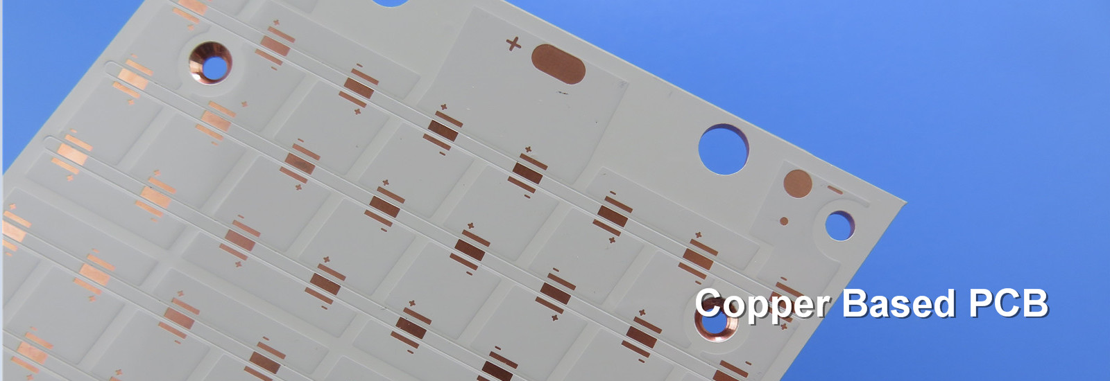
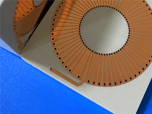
This custom double-sided RF circuit uses TFA294, an aerospace-grade PTFE-ceramic composite substrate formulated without woven glass fibres. Measuring 49mm × 90.3mm, the board maintains a strict ±0.15mm dimensional tolerance and features OSP surface protection. Neither solder mask nor silkscreen is applied to either side of the circuit. The design utilises through-hole architecture exclusively, with no blind vias. It supports routing down to 6/7 mil minimum trace and space, alongside a 0.35mm minimum hole diameter. Outer copper layers are plated to a 1oz finished weight, and 20 μm via plating delivers dependable electrical connections. The layout accommodates 16 component locations, 31 total pads and only 7 vias spread across two electrical nets, creating a neat, compact RF footprint. Every completed circuit undergoes full electrical continuity testing prior to dispatch and complies with IPC-Class-2 quality benchmarks. Gerber RS-274-X artwork files are accepted for fabrication, and shipments can be arranged for clients across the globe.
PCB Specification
High-frequency microwave circuits demand tightly controlled physical dimensions and manufacturing parameters to preserve signal integrity. The table below compiles all physical specifications, fabrication constraints and surface treatment details for this TFA294 circuit for your review.
| Item | Details |
| Base Material | TFA294 |
| Layer Count | 2 Layers |
| Board Dimensions | 49mm x 90.3mm, +/-0.15mm |
| Minimum Trace/Space | 6/7 mils |
| Minimum Hole Size | 0.35mm |
| Blind Vias | None |
| Finished Board Thickness | 2.1 mm |
| Finished Cu Weight | 1oz (1.4 mils) outer layers |
| Via Plating Thickness | 20 μm |
| Surface Finish | OSP |
| Top Silkscreen | No |
| Bottom Silkscreen | No |
| Top Solder Mask | No |
| Bottom Solder Mask | No |
| Pre-Shipment Test | 100% Electrical test |
PCB Stack-up
A board’s stack-up directly shapes impedance response and RF performance at microwave frequencies. The table below outlines the layer configuration of this two-layer rigid PCB, listing copper foil and core substrate from top to bottom.
| Layer | Material / Copper | Thickness |
| Copper_layer_1 | Copper | 35 μm |
| Core | TFA294 Core | 2.03 mm (80mil) |
| Copper_layer_2 | Copper | 35 μm |
![]()
PCB Statistics
Layout statistics illustrate circuit complexity and the distribution of pads and vias extracted directly from the submitted design artwork. This table summarises key layout metrics exported from the PCB design file.
| Item | Quantity |
| Components | 16 |
| Total Pads | 31 |
| Thru Hole Pads | 18 |
| Top SMT Pads | 13 |
| Bottom SMT Pads | 0 |
| Vias | 7 |
| Nets | 2 |
Introduction of TFA series
TFA-series laminates are PTFE ceramic composite dielectrics. Unlike traditional high-frequency substrates, these materials skip the conventional prepreg production method that soaks glass fabric in resin. Instead, proprietary manufacturing forms the base sheets, which are then bonded together via a specialised lamination process. The material delivers strong electrical, thermal and mechanical performance, making it an aerospace-grade high-frequency alternative to comparable imported substrates.
No woven glass fibre is present within the TFA composite matrix. Uniform nano-ceramic fillers are dispersed throughout the PTFE resin, which eliminates glass weave distortion that interferes with electromagnetic wave propagation. The material maintains stable frequency response paired with low dielectric loss. Its X/Y/Z anisotropy is greatly minimised, boasting a low thermal expansion coefficient that closely matches copper foil and steady dielectric performance across temperature shifts. Four Dk grades are available in this product family: 2.94, 3.0, 6.15 and 10.2, corresponding to part numbers TFA294, TFA300, TFA615 and TFA1020.
![]()
Features of TFA294
Typical Applications
Quality & Production Information
Gerber RS-274-X artwork files are supported for manufacturing. Fabrication adheres to IPC-Class-2 standards, with global delivery options available.
Conclusion
This two-layer TFA294 PCB combines ultra-stable dielectric behaviour and robust thermal characteristics for demanding high-frequency RF systems. The glass-free construction removes signal distortion caused by glass weave effects, while its copper-matched CTE and minimal TCDK preserve consistent performance through wide temperature fluctuations. OSP surface finish provides a cost-effective, clean metallisation surface ideal for assembly, with mandatory electrical testing completed before shipment. Manufactured to aerospace-grade material standards, this board acts as a reliable custom circuit solution for radar, satellite and airborne RF hardware, suitable for prototype validation and mass production shipped worldwide.