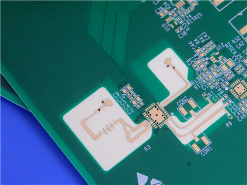
This 4-layer high-frequency hybrid PCB features a composite substrate combining RO4003C and FR4 (TG175), striking an optimal balance between high-frequency performance and cost-efficiency. Manufactured in strict compliance with IPC-3 standards, it boasts precise structural control and reliable process quality, making it ideal for high-frequency signal transmission scenarios that demand stable performance and moderate cost. Integrating excellent electrical properties, mechanical stability and process compatibility, this product can meet the application needs of a wide range of electronic devices.
PCB Specifications
| Specification Item |
Technical Specification |
| Layer Configuration |
4-Layer Rigid PCB |
| Base Substrate Material |
RO4003C + FR4 (TG175) (Hybrid Substrate) |
| Finished Board Thickness |
1.4 mm |
| Board Dimensions |
200mm × 115mm (per unit), 1 piece per unit |
| Copper Weight (Inner Layers) |
0.5 oz |
| Finished Copper Weight |
1 oz |
| Surface Finish |
Immersion Gold (2 U") |
| Solder Mask & Silkscreen |
Green Solder Mask with White Silkscreen Text |
| Plated Through-Hole (PTH) Copper Thickness |
25 μm |
| Quality Standard |
IPC-3 Compliant |
| Special Process |
Controlled Depth Slot (Depth tolerance is strictly maintained within ±0.05mm with real-time laser ranging feedback; slot wall angle is 85°-90° achieved via mechanical milling). |
PCB Stack-Up Structure (From Top to Bottom)
| Layer/Component |
Thickness |
| L1 Copper (Top Layer) |
0.035 mm |
| RO4003C Core |
0.203 mm |
| L2 Copper (Inner Layer 1) |
0.018 mm |
| Prepreg 2113 |
0.102 mm |
| FR-4 Substrate (TG175) |
0.6 mm |
| Prepreg 2113 |
0.102 mm |
| L3 Copper (Inner Layer 2) |
0.018 mm |
| Core FR-4 (TG175) |
0.203 mm |
| L4 Copper (Bottom Layer) |
0.035 mm |

RO4003C Substrate Introduction
RO4003C is a proprietary glass cloth-reinforced, ceramic-filled hydrocarbon composite material developed by Rogers Corporation. It merges the electrical performance of PTFE/glass cloth with the processability of epoxy resin/glass, eliminating the need for special through-hole treatments or operational procedures—setting it apart from PTFE microwave materials. Non-brominated and not UL 94 V-0 compliant, it can be replaced with RO4835 or RO4350B laminates for applications requiring flame retardancy. Its stable dielectric properties and cost-effectiveness make it widely used in high-frequency PCB manufacturing.
Application Fields
-High-frequency communication equipment: Microwave antennas, RF amplifiers, and signal transceivers.
-Automotive electronics: On-board radar, in-vehicle communication modules, and GPS navigation systems.
-Consumer electronics: High-frequency wireless devices, smart wearables, and high-speed data transmission equipment.
-Industrial equipment: Test and measurement instruments, and industrial control systems requiring stable high-frequency signals.
-Aerospace and defense: Low-cost microwave components and airborne communication equipment.
Processing Points
Processing Compatibility: Compatible with standard FR-4 equipment/processes and most tooling systems; recommended slotted pins, multiline tooling and post-etch punching; works with most photoresists and standard DES systems.
Storage: Store at 10-32°C (50-90°F); adopt first-in-first-out inventory and track material lot numbers.
Inner Layer Preparation: Thinner cores need chemical surface preparation, thicker cores allow mechanical scrub; use copper oxide or alternative process for multi-layer bonding.
Drilling: Avoid speeds >500 SFM; chip loads vary by drill diameter; standard geometry drills preferred; hole wall roughness 8-25 μm, hit counts based on PTH inspection.
PTH Processing: Surface preparation depends on material thickness; desmear usually unnecessary for double-sided boards (may be needed for multi-layer); no special metallization treatment; 0.00025” copper flash for high aspect ratio holes; no RO4003C etchback.
Copper Plating: Compatible with standard plating and SES processes; preserve post-etch surface for solder mask adhesion.
Final Finishes: Compatible with OSP, HASL and most chemical/electroplated finishes.
Routing: Use carbide tools; etch copper off routing path; circuits can be individualized via multiple methods (dicing, sawing, etc.).
Multi-Layer Bonding: Compatible with various adhesive systems; follow adhesive guidelines for bond parameters.
High-Frequency Hybrid PCB (Hybrid PCB)
A high-frequency hybrid PCB is a composite printed circuit board that integrates two or more different substrate materials (typically high-frequency and standard substrates) into a single PCB structure. It combines the strengths of each substrate: high-frequency substrates (e.g., RO4003C) are used in areas requiring high-frequency signal transmission to ensure signal integrity, while standard substrates (e.g., FR4) are used in areas needing only basic electrical connections to control production costs. This product is a typical high-frequency hybrid PCB, combining the RO4003C high-frequency substrate with the FR4 (TG175) standard substrate.
Advantages
Cost-Effectiveness: Eliminates the high cost of using high-frequency substrates for the entire board. By utilizing standard substrates in non-high-frequency areas, it significantly reduces overall PCB production costs while maintaining high-frequency performance.
Optimal Performance Matching: High-frequency areas use high-frequency substrates with low Df and stable Dk, effectively reducing signal loss, crosstalk, and delay to ensure stable high-frequency signal transmission; standard areas use FR4 substrates to meet basic electrical and mechanical requirements.
Process Compatibility: Can be processed via standard PCB production processes without the need for special production lines, facilitating mass production and improving efficiency.
Flexible Design: Can be flexibly designed based on the signal transmission requirements of different PCB areas, achieving the optimal balance of performance and cost to adapt to the design needs of various complex electronic products.
Disadvantages
Complex Design: The design process must account for differences in parameters such as thermal expansion coefficient (CTE) and dielectric properties between different substrates, increasing the difficulty of PCB layout and stack-up design.
Strict Lamination Requirements: Due to differences in the physical and chemical properties of various substrates, lamination process parameters (temperature, pressure, time) must be strictly controlled to avoid defects such as delamination and warpage between substrates.
Higher Processing Precision Requirements: Material property differences may lead to uneven processing (e.g., drilling, etching), requiring higher processing precision and increasing quality control difficulty.
Higher Technical Threshold: Requires manufacturers to have extensive experience in hybrid substrate processing, including material selection, process parameter adjustment, and defect control, raising the production technical threshold.

 Your message must be between 20-3,000 characters!
 English