| MOQ: | 1PCS |
| Price: | USD9.99-99.99 |
| Standard Packaging: | Vacuum bags+Cartons |
| Delivery Period: | 8-9 working days |
| Payment Method: | T/T |
| Supply Capacity: | 5000PCS per month |
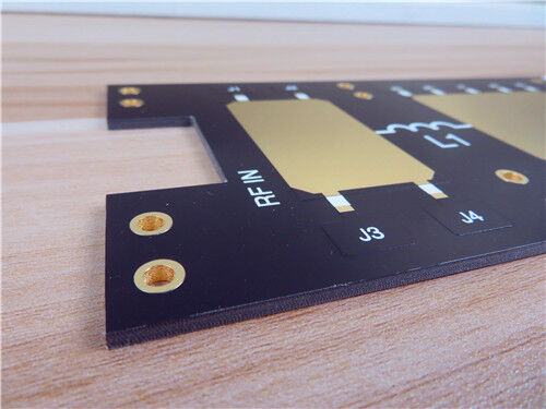
This two-layer high-frequency rigid PCB uses F4BM275 PTFE laminate and carries ENIG plating. The surface treatment is set up so white silkscreen and black solder mask only sit on the top copper. The bottom remains open, with no print and no solder mask applied. It works well for RF users building microwave modules, radar hardware, phase shifters, power dividers, couplers, feed networks, phased array antennas, satellite links and base station antenna systems, especially where strict PIM performance is not required.
PCB Specifications
| Item | Details |
| Base material | F4BM275 |
| Layer count | 2 layers |
| Board dimensions | 38.5 mm × 77 mm per piece, tolerance ±0.15 mm |
| Minimum Trace / Space | 4 / 6 mils |
| Minimum Hole Size | 0.4 mm |
| Blind vias | None |
| Finished board thickness | 1.6 mm |
| Finished copper weight | 1 oz (1.4 mils) outer layers |
| Via plating thickness | 20 μm |
| Surface finish | ENIG |
| Top Silkscreen | White |
| Bottom Silkscreen | No |
| Top Solder Mask | Black |
| Bottom Solder Mask | No |
| Pre-shipment check | 100% electrical test |
Gerber RS-274-X is the artwork format we accept. Every batch follows IPC-Class-2 requirements, and we ship these bare boards to customers anywhere in the world.
PCB Stack-up
This simple two-layer build has one solid F4BM275 core sandwiched between two copper sheets.
| Layer | Material & Thickness |
| Copper_layer_1 | 35 μm |
| F4BM275 Core | 1.524 mm (60 mil) |
| Copper_layer_2 | 35 μm |
PCB Statistics
| Item | Quantity |
| Components | 34 |
| Total Pads | 59 |
| Thru Hole Pads | 36 |
| Top SMT Pads | 23 |
| Bottom SMT Pads | 0 |
| Vias | 32 |
| Nets | 4 |
![]()
About F4BM Laminate
F4BM laminates are made from fiberglass cloth, PTFE resin and PTFE film. All raw materials go through precise mixing and pressing under tight process control. Compared with standard F4B, this material delivers better electrical performance. It offers more dielectric constant choices, lower dielectric loss, higher insulation resistance and greater stability over time. It serves as a reliable substitute for similar imported laminates.
F4BM and F4BME share the same dielectric core, yet they use different copper foil. F4BM pairs with ED copper foil and fits projects without tight PIM demands. F4BME uses reverse-treated foil instead; it delivers better PIM behaviour, cleaner line definition and less conductor loss.
Adjusting the proportion between PTFE and fiberglass cloth lets us hit the target dielectric constant. This keeps signal loss low while holding dimensions steady. Grades with a higher dielectric constant contain more fiberglass. They hold shape better, expand less under heat and show milder temperature drift, though dielectric loss rises slightly.
![]()
Key Features of F4BM275
General Series Features
Typical Applications
This F4BM275 RF Circuit board is a practical pick if you are sourcing affordable PTFE circuit stock without strict PIM limits. Its electrical response stays consistent even when temperature shifts, and all production runs follow IPC-Class-2 standards. We take orders for small prototype quantities as well as larger repeat runs, with delivery available worldwide. Send your Gerber files, and our team will work up a quote. You can write anytime to ask about lead time or pricing for bare microwave and satellite circuit boards.
![]()
| MOQ: | 1PCS |
| Price: | USD9.99-99.99 |
| Standard Packaging: | Vacuum bags+Cartons |
| Delivery Period: | 8-9 working days |
| Payment Method: | T/T |
| Supply Capacity: | 5000PCS per month |
This two-layer high-frequency rigid PCB uses F4BM275 PTFE laminate and carries ENIG plating. The surface treatment is set up so white silkscreen and black solder mask only sit on the top copper. The bottom remains open, with no print and no solder mask applied. It works well for RF users building microwave modules, radar hardware, phase shifters, power dividers, couplers, feed networks, phased array antennas, satellite links and base station antenna systems, especially where strict PIM performance is not required.
PCB Specifications
| Item | Details |
| Base material | F4BM275 |
| Layer count | 2 layers |
| Board dimensions | 38.5 mm × 77 mm per piece, tolerance ±0.15 mm |
| Minimum Trace / Space | 4 / 6 mils |
| Minimum Hole Size | 0.4 mm |
| Blind vias | None |
| Finished board thickness | 1.6 mm |
| Finished copper weight | 1 oz (1.4 mils) outer layers |
| Via plating thickness | 20 μm |
| Surface finish | ENIG |
| Top Silkscreen | White |
| Bottom Silkscreen | No |
| Top Solder Mask | Black |
| Bottom Solder Mask | No |
| Pre-shipment check | 100% electrical test |
Gerber RS-274-X is the artwork format we accept. Every batch follows IPC-Class-2 requirements, and we ship these bare boards to customers anywhere in the world.
PCB Stack-up
This simple two-layer build has one solid F4BM275 core sandwiched between two copper sheets.
| Layer | Material & Thickness |
| Copper_layer_1 | 35 μm |
| F4BM275 Core | 1.524 mm (60 mil) |
| Copper_layer_2 | 35 μm |
PCB Statistics
| Item | Quantity |
| Components | 34 |
| Total Pads | 59 |
| Thru Hole Pads | 36 |
| Top SMT Pads | 23 |
| Bottom SMT Pads | 0 |
| Vias | 32 |
| Nets | 4 |
![]()
About F4BM Laminate
F4BM laminates are made from fiberglass cloth, PTFE resin and PTFE film. All raw materials go through precise mixing and pressing under tight process control. Compared with standard F4B, this material delivers better electrical performance. It offers more dielectric constant choices, lower dielectric loss, higher insulation resistance and greater stability over time. It serves as a reliable substitute for similar imported laminates.
F4BM and F4BME share the same dielectric core, yet they use different copper foil. F4BM pairs with ED copper foil and fits projects without tight PIM demands. F4BME uses reverse-treated foil instead; it delivers better PIM behaviour, cleaner line definition and less conductor loss.
Adjusting the proportion between PTFE and fiberglass cloth lets us hit the target dielectric constant. This keeps signal loss low while holding dimensions steady. Grades with a higher dielectric constant contain more fiberglass. They hold shape better, expand less under heat and show milder temperature drift, though dielectric loss rises slightly.
![]()
Key Features of F4BM275
General Series Features
Typical Applications
This F4BM275 RF Circuit board is a practical pick if you are sourcing affordable PTFE circuit stock without strict PIM limits. Its electrical response stays consistent even when temperature shifts, and all production runs follow IPC-Class-2 standards. We take orders for small prototype quantities as well as larger repeat runs, with delivery available worldwide. Send your Gerber files, and our team will work up a quote. You can write anytime to ask about lead time or pricing for bare microwave and satellite circuit boards.
![]()