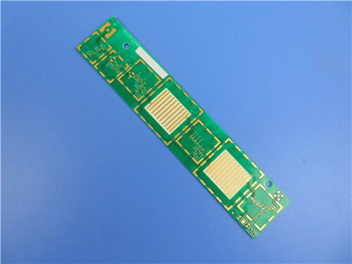
This 8-layer high-frequency hybrid PCB adopts a composite substrate structure, with 10mil RO4350B high-frequency substrate on the top and bottom layers, and FR-4 Tg180 substrate in the middle. It perfectly balances excellent high-frequency signal performance and cost-effectiveness, strictly complies with IPC Class 3 quality standards, and is equipped with special processes such as metal edge wrapping, blind/buried vias and resin plugging. With precise structural control and reliable process quality, it is suitable for high-frequency, high-precision electronic equipment scenarios requiring stable signal transmission.
PCB Specifications
| Specification Item |
Technical Specification |
| Layer Configuration |
8-Layer Rigid PCB |
| Base Substrate Material |
Top Layer: 10mil RO4350B; Middle Layer: FR-4 Tg180; Bottom Layer: 10mil RO4350B (Hybrid Substrate) |
| Finished Board Thickness |
1.553 mm |
| Board Dimensions |
120mm × 30mm (per unit), 1 piece per unit |
| Copper Weight (Inner Layers) |
1 oz |
| Copper Weight (Outer Layers) |
1 oz |
| Surface Finish |
ENIG (Electroless Nickel Immersion Gold) |
| Solder Mask & Silkscreen |
Green Solder Mask with White Silkscreen Text |
| Plated Through-Hole (PTH) Copper Thickness |
25 μm |
| Quality Standard |
IPC Class 3 Compliant |
| Special Processes |
1. Metal Edge Wrapping; 2. Blind Vias (Layer 1-2), Buried Vias (Layer 5-6); 3. Resin Plugging |
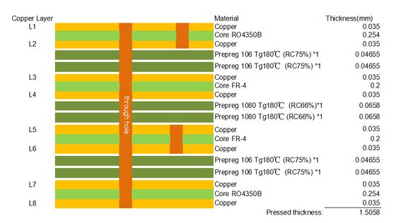
PCB Stack-Up Structure (From Top to Bottom)
| Layer/Component |
Thickness |
| L1 Copper (Top Outer Layer) |
0.035 mm (1 oz) |
| RO4350B Core (Top Layer) |
0.254 mm (10 mil) |
| L2 Copper (Inner Layer 1) |
0.035 mm (1 oz) |
| Prepreg |
0.04655mm |
| Prepreg |
0.04655mm |
| L3 Copper (Inner Layer 2) |
0.035 mm (1 oz) |
| FR-4 Tg180 Core (Middle Layer) |
0.2mm |
| L4 Copper (Inner Layer 3) |
0.035 mm (1 oz) |
| Prepreg |
0.0658mm |
| Prepreg |
0.0658mm |
| L5 Copper (Inner Layer 4) |
0.035 mm (1 oz) |
| FR-4 |
0.2mm |
| L6 Copper (Inner Layer 5) |
0.035 mm (1 oz) |
| Prepreg |
0.04655mm |
| Prepreg |
0.04655mm |
| L7 Copper (Inner Layer 6) |
0.035 mm (1 oz) |
| RO4350B Core (Bottom Layer) |
0.254 mm (10 mil) |
| L8 Copper (Bottom Outer Layer) |
0.035 mm (1 oz) |

RO4350B Substrate Introduction
RO4350B is a high-performance glass-reinforced hydrocarbon/ceramic composite substrate, specially designed for high-frequency, high-speed circuit applications. It features stable dielectric properties, low dissipation factor, and excellent mechanical and thermal stability, making it widely used in various high-frequency electronic products. The material is compatible with standard PCB processing processes, easy to process, and can effectively ensure signal integrity in high-frequency transmission scenarios.
RO4350B Key Features
-Low dissipation factor (Df) and stable dielectric constant (Dk), ensuring minimal high-frequency signal loss
-Low moisture absorption, maintaining stable electrical performance in different environmental conditions
-Excellent mechanical strength and dimensional stability, suitable for multi-layer PCB lamination
-Good compatibility with standard PCB processing equipment and processes, reducing production costs
-Excellent chemical resistance, resistant to common solvents and reagents used in PCB processing
RO4350B Application Fields
-High-frequency communication equipment: RF modules, microwave antennas, signal transceivers and point-to-point digital radio antennas
-Automotive electronics: On-board radar systems, in-vehicle communication modules
-Aerospace and defense: radar systems, missile guidance systems
-Test and measurement instruments: High-frequency test equipment, signal analyzers
-Consumer electronics: High-speed wireless routers, smart wearables, high-frequency wireless devices
RO4350B Processing Points
Inner Layer Preparation
Tooling: RO4350B laminates are compatible with many pinned and pinless tooling systems. Slotted pins, a multiline tooling format, and post-etch punching are generally recommended to meet most registration requirements.
Surface Preparation: Thinner RO4350B cores should be prepared using a chemical process (cleaning, micro-etching, water rinsing, drying); thicker cores are compatible with mechanical scrub systems. It is compatible with most liquid and dry film photoresists and can be processed via standard develop, etch, and strip (DES) systems.
Oxide Treatment: RO4350B cores can be processed through any copper oxide or oxide alternative process for multi-layer bonding, with the optimal treatment selected based on prepreg/adhesive system guidelines.
Drilling Requirements
Standard entry (aluminum or thin pressed phenolic) and exit (pressed phenolic or fiber board) materials are suitable for drilling RO4350B cores or bonded assemblies.
Drilling speeds greater than 500 surface feet per minute (SFM) should be avoided. Chip loads >0.002”/” are recommended for mid-range and large diameter tools, while <0.002”/” for small diameter drills (<0.0135”).
Standard geometry drills are preferred for efficient debris evacuation. Hit counts should be based on PTH inspection. Drill wear is accelerated, but hole wall quality (8-25 μm roughness) is determined by ceramic powder size distribution.
Multi-Layer Bonding
RO4350B laminates are compatible with many thermosetting and thermoplastic adhesive systems. Bond cycle parameters should follow the adhesive system’s guidelines.
Blind Vias and Buried Vias
Blind Vias: Holes that only penetrate from the surface of the PCB (one side) to a specified inner layer, without passing through the entire board. This product is designed with blind vias between Layer 1 and Layer 2, which only connect the top outer layer and the first inner layer.
Buried Vias: Holes that are completely located inside the PCB, connecting two or more inner layers without exposing the surface of the board. This product is designed with buried vias between Layer 5 and Layer 6, which only connect the fifth and sixth inner layers.
Why Use Blind Vias & Buried Vias
Improve Signal Integrity: Blind vias and buried vias shorten the signal transmission path, reduce signal delay, crosstalk and loss, which is crucial for high-frequency signal transmission.
Save Board Space: Compared with through holes, blind vias and buried vias do not occupy the surface space of the PCB, allowing for more dense component layout and improving the integration of the PCB.
Enhance PCB Reliability: Avoiding through holes penetrating the entire board reduces the risk of board warpage and layer separation, and resin plugging further protects the holes from moisture and contamination.
Optimize Assembly Process: Resin-plugged blind vias and buried vias ensure the flatness of the PCB surface, facilitating the soldering of surface-mounted components (SMD) and improving assembly accuracy.

 Your message must be between 20-3,000 characters!
 English