| MOQ: | 1PCS |
| Price: | USD9.99-99.99 |
| Standard Packaging: | Vacuum bags+Cartons |
| Delivery Period: | 8-9 working days |
| Payment Method: | T/T |
| Supply Capacity: | 5000PCS per month |
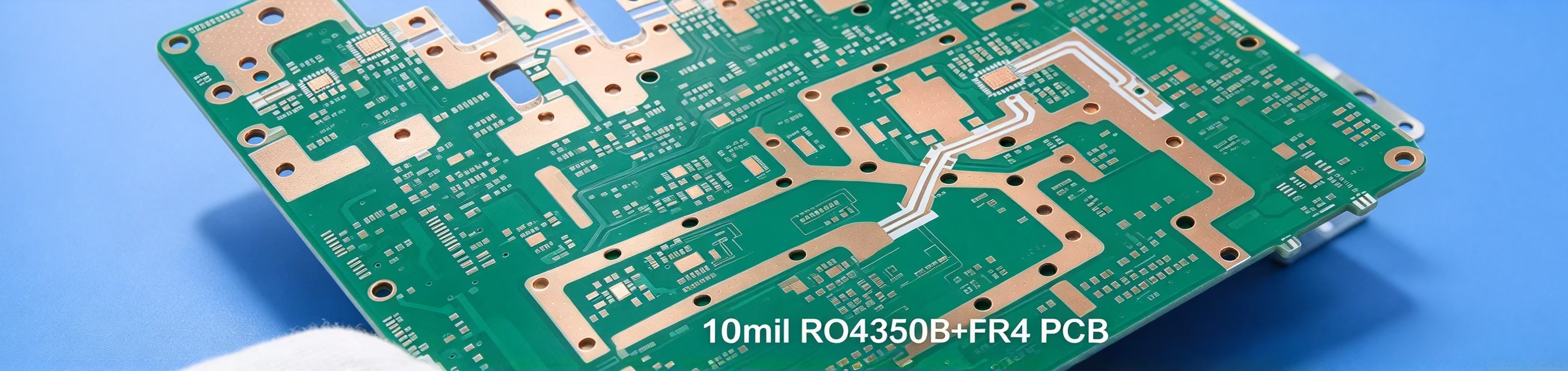
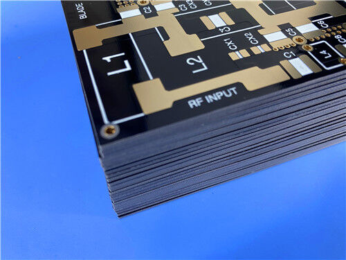
This two-layer rigid PCB adopts F4BTMS350 ceramic filled PTFE substrate, with EPIG as the surface finish. It carries green solder mask on the top while the bottom remains free of solder mask, and white silkscreen is applied only to the top side. This board serves microwave and radio frequency work, suited for aerospace hardware, radar and satellite communication systems. All fabrication parameters are tightly controlled to satisfy strict project requirements. Every finished PCB passes full electrical inspection before shipment, built to IPC-Class-2 and available for delivery worldwide.
PCB Specifications
| Item | Details |
| Base material | F4BTMS350 ceramic filled PTFE substrate |
| Board dimensions | 38.35 mm × 101.66 mm, ±0.15 mm, 1 piece |
| Minimum Trace / Space | 6 / 9 mils |
| Minimum Hole Size | 0.4 mm |
| Blind vias | None |
| Finished board thickness | 1.3 mm |
| Outer finished copper | 1 oz (1.4 mils) |
| Via plating thickness | 20 μm |
| Surface finish | EPIG |
| Top silkscreen | White |
| Bottom silkscreen | None |
| Top solder mask | Green |
| Bottom solder mask | None |
| Pre-shipment test | 100% electrical test |
Stack-up
This is a straightforward two-layer construction. A single F4BTMS350 core sits between two copper layers. There are no complex lamination steps or embedded materials, which keeps electrical performance predictable.
| Layer | Specification |
| Copper_layer_1 | 35 μm |
| Core | F4BTMS350, 1.27 mm (50 mil) |
| Copper_layer_2 | 35 μm |
PCB Statistics
These figures come directly from the supplied Gerber files. They show the pad, via and net counts used to assess production feasibility.
| Item | Quantity |
| Components | 87 |
| Total Pads | 69 |
| Thru Hole Pads | 41 |
| Top SMT Pads | 28 |
| Bottom SMT Pads | 0 |
| Vias | 13 |
| Nets | 6 |
![]()
F4BTMS Series Introduction
The F4BTMS series is an upgraded version of F4BTM. Updates to the material formula and manufacturing process bring clear performance gains and a wider selection of dielectric constants. It is a high-reliability substrate built for aerospace use and can replace equivalent imported materials.
The resin system mixes PTFE with evenly distributed nano-ceramic fillers and a small amount of ultra-thin, ultra-fine fiberglass cloth. This cuts down the glass fiber effect that disturbs electromagnetic waves. Dielectric loss goes down, dimensional stability improves, and anisotropy across X, Y and Z directions is reduced. The material works reliably at higher frequencies, with better dielectric strength and thermal conductivity. It also features low thermal expansion and steady dielectric characteristics over changing temperatures.
RTF low-roughness copper foil is standard for this material line. It reduces conductor loss while maintaining good peel strength, and works with both copper and aluminum base options. It can be processed using regular PTFE fabrication methods. Its solid mechanical properties support multilayer and backplane production, and it handles dense hole layouts and fine traces well.
![]()
| Product Technical Parameters | Product Models & Data Sheet | ||
| Product Features | Test Conditions | Unit | F4BTMS350 |
| Dielectric Constant (Typical) | 10GHz | / | 3.50 |
| Dielectric Constant Tolerance | / | / | ±0.05 |
| Dielectric Constant (Design) | 10GHz | / | 3.50 |
| Loss Tangent (Typical) | 10GHz | / | 0.0016 |
| 20GHz | / | 0.0019 | |
| 40GHz | / | 0.0024 | |
| Dielectric Constant Temperature Coefficient | -55 º~150ºC | PPM/℃ | -39 |
| Peel Strength | 1 OZ RTF copper | N/mm | >1.2 |
| Volume Resistivity | Standard Condition | MΩ.cm | ≥1×10^8 |
| Surface Resistivity | Standard Condition | MΩ | ≥1×10^8 |
| Electrical Strength (Z direction) | 5KW,500V/s | KV/mm | >42 |
| Breakdown Voltage (XY direction) | 5KW,500V/s | KV | >55 |
| Coefficientof Thermal Expansion (X, Y direction) | -55 º~288ºC | ppm/ºC | 10, 12 |
| Coefficientof Thermal Expansion (Z direction) | -55 º~288ºC | ppm/ºC | 20 |
| Thermal Stress | 260℃, 10s,3 times | / | No delamination |
| Water Absorption | 20±2℃, 24 hours | % | 0.03 |
| Density | Room Temperature | g/cm3 | 2.3 |
| Long-Term Operating Temperature | High-Low Temperature Chamber | ℃ | -55~+260 |
| Thermal Conductivity | Z direction | W/(M.K) | 0.6 |
| Flammability | / | UL-94 | V-0 |
| Material Composition | / | / | PTFE,Ultra-thin and ultra-fine fiberglass, ceramics. |
Features
Applications
With consistent high-frequency response, solid thermal performance and low outgassing, F4BTMS350 fits demanding microwave circuits where phase stability and long-term reliability matter. Submit the relevant files to get a quote, and pricing will be based on the provided Gerber data and production requirements.
Available Panel Size
305×460mm(12×18=) 460×610mm(18×24=) 610×920mm(24×36=)
F4BTMS350 Dielectric thickness and tolerance
| Thickness mm(mil) | Tolerance mm(mil) | Thickness mm(mil) | Tolerance mm(mil) |
| 0.254mm(10mil) | ±0.02mm(1.0mil) | 1.575mm(62mil) | ±0.06mm(2.5mil) |
| 0.508mm(20mil) | ±0.03mm(1.19mil) | 2.03mm(80mil) | ±0.08mm(3.2mil) |
| 0.635mm(25mil) | ±0.04mm(1.58mil) | 2.54mm(100mil) | ±0.10mm(4.0mil) |
| 0.762mm(30mil) | ±0.04mm(1.58mil) | 3.175mm(125mil) | ±0.13mm(5.0mil) |
| 0.787mm(30.1mil) | ±0.04mm(1.58mil) | 4.06mm(160mil) | ±0.18mm(7.0mil) |
| 1.016mm(40mil) | ±0.05mm(2.0mil) | 5.08mm(200mil) | ±0.20mm(8.0mil) |
| 1.270mm(50mil) | ±0.05mm(2.0mil) | 6.35mm(250mil) | ±0.25mm(10mil) |
| 1.50mm(59mil) | ±0.06mm(2.5mil) | ||
| 1.524mm(60mil) | ±0.06mm(2.5mil) |
![]()
![]()
| MOQ: | 1PCS |
| Price: | USD9.99-99.99 |
| Standard Packaging: | Vacuum bags+Cartons |
| Delivery Period: | 8-9 working days |
| Payment Method: | T/T |
| Supply Capacity: | 5000PCS per month |
This two-layer rigid PCB adopts F4BTMS350 ceramic filled PTFE substrate, with EPIG as the surface finish. It carries green solder mask on the top while the bottom remains free of solder mask, and white silkscreen is applied only to the top side. This board serves microwave and radio frequency work, suited for aerospace hardware, radar and satellite communication systems. All fabrication parameters are tightly controlled to satisfy strict project requirements. Every finished PCB passes full electrical inspection before shipment, built to IPC-Class-2 and available for delivery worldwide.
PCB Specifications
| Item | Details |
| Base material | F4BTMS350 ceramic filled PTFE substrate |
| Board dimensions | 38.35 mm × 101.66 mm, ±0.15 mm, 1 piece |
| Minimum Trace / Space | 6 / 9 mils |
| Minimum Hole Size | 0.4 mm |
| Blind vias | None |
| Finished board thickness | 1.3 mm |
| Outer finished copper | 1 oz (1.4 mils) |
| Via plating thickness | 20 μm |
| Surface finish | EPIG |
| Top silkscreen | White |
| Bottom silkscreen | None |
| Top solder mask | Green |
| Bottom solder mask | None |
| Pre-shipment test | 100% electrical test |
Stack-up
This is a straightforward two-layer construction. A single F4BTMS350 core sits between two copper layers. There are no complex lamination steps or embedded materials, which keeps electrical performance predictable.
| Layer | Specification |
| Copper_layer_1 | 35 μm |
| Core | F4BTMS350, 1.27 mm (50 mil) |
| Copper_layer_2 | 35 μm |
PCB Statistics
These figures come directly from the supplied Gerber files. They show the pad, via and net counts used to assess production feasibility.
| Item | Quantity |
| Components | 87 |
| Total Pads | 69 |
| Thru Hole Pads | 41 |
| Top SMT Pads | 28 |
| Bottom SMT Pads | 0 |
| Vias | 13 |
| Nets | 6 |
![]()
F4BTMS Series Introduction
The F4BTMS series is an upgraded version of F4BTM. Updates to the material formula and manufacturing process bring clear performance gains and a wider selection of dielectric constants. It is a high-reliability substrate built for aerospace use and can replace equivalent imported materials.
The resin system mixes PTFE with evenly distributed nano-ceramic fillers and a small amount of ultra-thin, ultra-fine fiberglass cloth. This cuts down the glass fiber effect that disturbs electromagnetic waves. Dielectric loss goes down, dimensional stability improves, and anisotropy across X, Y and Z directions is reduced. The material works reliably at higher frequencies, with better dielectric strength and thermal conductivity. It also features low thermal expansion and steady dielectric characteristics over changing temperatures.
RTF low-roughness copper foil is standard for this material line. It reduces conductor loss while maintaining good peel strength, and works with both copper and aluminum base options. It can be processed using regular PTFE fabrication methods. Its solid mechanical properties support multilayer and backplane production, and it handles dense hole layouts and fine traces well.
![]()
| Product Technical Parameters | Product Models & Data Sheet | ||
| Product Features | Test Conditions | Unit | F4BTMS350 |
| Dielectric Constant (Typical) | 10GHz | / | 3.50 |
| Dielectric Constant Tolerance | / | / | ±0.05 |
| Dielectric Constant (Design) | 10GHz | / | 3.50 |
| Loss Tangent (Typical) | 10GHz | / | 0.0016 |
| 20GHz | / | 0.0019 | |
| 40GHz | / | 0.0024 | |
| Dielectric Constant Temperature Coefficient | -55 º~150ºC | PPM/℃ | -39 |
| Peel Strength | 1 OZ RTF copper | N/mm | >1.2 |
| Volume Resistivity | Standard Condition | MΩ.cm | ≥1×10^8 |
| Surface Resistivity | Standard Condition | MΩ | ≥1×10^8 |
| Electrical Strength (Z direction) | 5KW,500V/s | KV/mm | >42 |
| Breakdown Voltage (XY direction) | 5KW,500V/s | KV | >55 |
| Coefficientof Thermal Expansion (X, Y direction) | -55 º~288ºC | ppm/ºC | 10, 12 |
| Coefficientof Thermal Expansion (Z direction) | -55 º~288ºC | ppm/ºC | 20 |
| Thermal Stress | 260℃, 10s,3 times | / | No delamination |
| Water Absorption | 20±2℃, 24 hours | % | 0.03 |
| Density | Room Temperature | g/cm3 | 2.3 |
| Long-Term Operating Temperature | High-Low Temperature Chamber | ℃ | -55~+260 |
| Thermal Conductivity | Z direction | W/(M.K) | 0.6 |
| Flammability | / | UL-94 | V-0 |
| Material Composition | / | / | PTFE,Ultra-thin and ultra-fine fiberglass, ceramics. |
Features
Applications
With consistent high-frequency response, solid thermal performance and low outgassing, F4BTMS350 fits demanding microwave circuits where phase stability and long-term reliability matter. Submit the relevant files to get a quote, and pricing will be based on the provided Gerber data and production requirements.
Available Panel Size
305×460mm(12×18=) 460×610mm(18×24=) 610×920mm(24×36=)
F4BTMS350 Dielectric thickness and tolerance
| Thickness mm(mil) | Tolerance mm(mil) | Thickness mm(mil) | Tolerance mm(mil) |
| 0.254mm(10mil) | ±0.02mm(1.0mil) | 1.575mm(62mil) | ±0.06mm(2.5mil) |
| 0.508mm(20mil) | ±0.03mm(1.19mil) | 2.03mm(80mil) | ±0.08mm(3.2mil) |
| 0.635mm(25mil) | ±0.04mm(1.58mil) | 2.54mm(100mil) | ±0.10mm(4.0mil) |
| 0.762mm(30mil) | ±0.04mm(1.58mil) | 3.175mm(125mil) | ±0.13mm(5.0mil) |
| 0.787mm(30.1mil) | ±0.04mm(1.58mil) | 4.06mm(160mil) | ±0.18mm(7.0mil) |
| 1.016mm(40mil) | ±0.05mm(2.0mil) | 5.08mm(200mil) | ±0.20mm(8.0mil) |
| 1.270mm(50mil) | ±0.05mm(2.0mil) | 6.35mm(250mil) | ±0.25mm(10mil) |
| 1.50mm(59mil) | ±0.06mm(2.5mil) | ||
| 1.524mm(60mil) | ±0.06mm(2.5mil) |
![]()
![]()