
|
Product Details:
Payment & Shipping Terms:
|
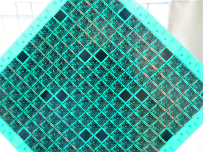
| Base Material: | FR-4 | Layer Count: | 6 Layers |
|---|---|---|---|
| PCB Thickness: | 0.6mm ±0.1 | PCB Size: | 100 X 103mm=1PCS |
| Solder Mask: | Green | Silkscreen: | NO |
| Copper Weight: | 1oz | Surface Finish: | Immersion Gold |
| High Light: | GPS Tracking Automotive Printed Circuit Board,0.6mm Automotive Printed Circuit Board,0.6mm 6 Layer PCB Board |
||
| PCB SIZE | 100 x 103mm=1PCS |
| BOARD TYPE | Multilayer PCB |
| Number of Layers | 6 layers |
| Surface Mount Components | YES |
| Through Hole Components | NO |
| LAYER STACKUP | copper ------- 18um(0.5oz)+plate TOP CS |
| 4mil prepreg | |
| copper ------- 18um(0.5oz) GND Plane | |
| 4mil FR-4 | |
| copper ------- 18um(0.5oz) PWR Plane | |
| 4mil prepreg | |
| copper ------- 18um(0.5oz) PWR Plane | |
| 4mil FR-4 | |
| copper ------- 18um(0.5oz) SIG | |
| 4mil prepreg | |
| copper ------- 18um(0.5oz) BOT PS | |
| TECHNOLOGY | |
| Minimum Trace and Space: | 3mil/3mil |
| Minimum / Maximum Holes: | 0.22/3.50mm |
| Number of Different Holes: | 25 |
| Number of Drill Holes: | 2315 |
| Number of Milled Slots: | 0 |
| Number of Internal Cutouts: | 0 |
| Impedance Control | no |
| BOARD MATERIAL | |
| Glass Epoxy: | FR-4, ITEQ IT140 TG>135, er<5.4 |
| Final foil external: | 1oz |
| Final foil internal: | 0.5oz |
| Final height of PCB: | 0.6mm ±0.1 |
| PLATING AND COATING | |
| Surface Finish | Immersion gold 0.025µm over 3µm Nickel (14.4% area) |
| Solder Mask Apply To: | TOP and Bottom, 12micron Minimum |
| Solder Mask Color: | Green, TAIYO PSR-2000 GT600D |
| Solder Mask Type: | LPSM |
| CONTOUR/CUTTING | Routing |
| MARKING | |
| Side of Component Legend | No silkscreen requried. |
| Colour of Component Legend | No silkscreen requried. |
| Manufacturer Name or Logo: | No silkscreen requried. |
| VIA | Plated through hole(PTH), Blind via and via capping on CS and PS, vias not be visible. |
| FLAMIBILITY RATING | UL 94-V0 Approval MIN. |
| DIMENSION TOLERANCE | |
| Outline dimension: | 0.0059" (0.15mm) |
| Board plating: | 0.0030" (0.076mm) |
| Drill tolerance: | 0.002" (0.05mm) |
| TEST | 100% Electrical Test prior shipment |
| TYPE OF ARTWORK TO BE SUPPLIED | email file, Gerber RS-274-X, PCBDOC etc |
| SERVICE AREA | Worldwide, Globally. |
| Serial NO. | Procedure | Item | Manufacturing capability | ||
| Large volume (S<100 m²) | Middle volume (S<10 m²) | Prototype(S<1m²) | |||
| 14 | Laminating | Tolerance of laminate thickness | ±10% PCB thick | ±10% PCB thick | ±8% PCB thick |
| 15 | Maximum laminate thickness | 4.0mm | 6.0mm | 7.0mm | |
| 16 | Laminate alignment accuracy | ≤±5 mil | ≤±4 mil | ≤±4 mil | |
| 17 | Drill (18um, 35um, 70um etc are finished copper. If not mentioned copper, finished 1oz is the default value ) | Min.drill bit diameter | 0.2 mm | 0.2 mm | 0.2 mm |
| 18 | Min.slot router diameter | 0.60 mm | 0.60 mm | 0.60 mm | |
| 19 | Min.tolerance of PTH slots | ±0.15mm | ±0.15mm | ±0.1mm | |
| 20 | Max.aspect ratio | 1:08 | 1:12 | 1:12 | |
| 21 | Hole tolerance | ±3mil | ±3mil | ±3mil | |
| 22 | Space of via to via | 6mil(same net),12mil(different net) | 6mil(same net),14mil(different net) | 4mil(same net),12mil(different net) | |
| 23 | Space of component hole to component hole | 12mil(same net),16mil(different net) | 12mil(same net),16mil(different net) | 10mil(same net),14mil(different net) | |
| 24 | Etching | Min.width of etching logo | 10mil(18um),12 mil (35um),12 mil(70um) | 8mil(18um),10mil(35um),12 mil(70um) | 6mil(18um),8 mil(35um),12mil(70um) |
| 25 | Etch factor | 1.6-2.2 | 1.6-2.2 | 1.6-2.2 | |
| 26 | Outer layer(18um, 35um, 70um etc are finished copper. If not mentioned copper, finished 1oz is the default value ) | Min.via pad diameter | 20mil | 16mil | 16mil |
| 27 | Min.BGA pad diameter | 12mil | 12mil | 10mil | |
| 28 | Min.track and spacing | 5/5mil(18um) | 4/4mil(18um) | 3/3.5mil(18um) | |
| 5/5mil(35um) | 4/4mil(35um) | 3/4mil(35um) | |||
| 7/9mil(70um) | 6/8mil(70um) | 6/7mil(70um) | |||
| 9/11mil(105um) | 8/10mil(105um) | 8/9mil(105um) | |||
| 13/13mil(140um) | 12/12mil(140um) | 12/11mil(140um) | |||
| 29 | Minimum grid | 10/10mil(35um) | 8/8mil(35um) | 4/8mil(35um) | |
| 30 | Min.space (conductor to pad, pad to pad) | 6mil(18um) | 5mil(18um) | 4mil(18um) | |
| 6mil(35um) | 5mil(35um) | 4mil(35um) | |||
| 9mil(70um) | 8mil(70um) | 7mil(70um) | |||
| 11mil(105um) | 10mil(105um) | 9mil(105um) | |||
| 13mil(140um) | 12mil(140um) | 11mil(140um) | |||
![]()
Contact Person: Ms. Ivy Deng
Tel: 86-755-27374946
Fax: 86-755-27374848

