Send Message
Home ProductsFR4 PCB Board

Single End Impedance 1.6mm Multilayer PCB Circuit Board 10 Layer PCB

China Bicheng Electronics Technology Co., Ltd certification
Kevin, Received and tested the boards - thanks very much. These are perfect, exactly what we needed. rgds Rich

—— Rich Rickett

Ruth, I got the PCB today, and they are just perfect. Please stay a little patience, my next order is coming soon. Kind regards from Hamburg Olaf

—— Olaf Kühnhold

Hi Natalie. It was perfect, I attach some pictures for your reference. And I send you next 2 projects to budget. Thanks a lot again

—— Sebastian Toplisek

Kevin, Thanks, they were perfectly made, and work well. As promised, here are the links for my latest project, using the PCBs you manufactured for me: Regards, Daniel

—— Daniel Ford

I'm Online Chat Now

Single End Impedance 1.6mm Multilayer PCB Circuit Board 10 Layer PCB

Single End Impedance 1.6mm Multilayer PCB Circuit Board 10 Layer PCB
Single End Impedance 1.6mm Multilayer PCB Circuit Board 10 Layer PCB Single End Impedance 1.6mm Multilayer PCB Circuit Board 10 Layer PCB Single End Impedance 1.6mm Multilayer PCB Circuit Board 10 Layer PCB Single End Impedance 1.6mm Multilayer PCB Circuit Board 10 Layer PCB Single End Impedance 1.6mm Multilayer PCB Circuit Board 10 Layer PCB

Large Image :  Single End Impedance 1.6mm Multilayer PCB Circuit Board 10 Layer PCB

Product Details:
Place of Origin: CHINA
Brand Name: Bicheng
Certification: UL, ISO9001, IATF16949
Model Number: BIC-475.V1.0
Payment & Shipping Terms:
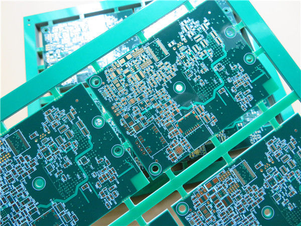
Minimum Order Quantity: 1PCS
Price: USD9.99-99.99
Packaging Details: Vacuum bags+Cartons
Delivery Time: 8-9 working days
Payment Terms: T/T
Supply Ability: 5000PCS per month
Detailed Product Description
Base Material: FR-4 Layer Count: 10 Layers
PCB Thickness: 1.6mm ±0.16 PCB Size: 199 X 170mm=4PCS
Solder Mask: Green Silkscreen: White
Copper Weight: 1oz Surface Finish: Immersion Gold
High Light:

10 Layer Multilayer PCB Circuit Board

,

1.6mm Multilayer PCB Circuit Board

,

1.6mm 10 Layer PCB

 
Differential Impedance Controlled PCB Single-End Impedance Circuit Board 10 Layer PCB Board Satellite systems
 
1.1 General description
This is a type of multilayer PCB built on FR-4 substrate with Tg 170°C for the application of Satellite systems with 10 layer copper. It's 1.6 mm thick with white silkscreen(Taiyo) on green solder mask (Taiyo) and immersion gold on pads. This is also an impedance controlled PCB with 50 ohm single-end impedance and 97 ohm with differential impedance control. The base material is from ITEQ supplying 4 up PCBs per panel. They're fabricated per IPC 6012 Class 2 using supplied Gerber data. Each 25 panels are packed for shipment.
 
1.2 Features and benifits
Lead free assemblies with a maximum reflow temperature of 260℃
SMT process is resistant to reflow soldering, resistant to rework.
The signal lines form a constant low impedance to the ground
Strict WIP inspection and monitoring as well as working instruction
UL, ISO14001, TS16949 certified
Hassle-free, one-to-one after-sales service
Delivery on time: >98%
 
Single End Impedance 1.6mm Multilayer PCB Circuit Board 10 Layer PCB 0
 
1.3 Applications
GPS Tracking Devices
GSM Signal Booster
Automotive dashboards
 
1.4 Parameter and data sheet
PCB SIZE 199 x 170mm=4PCS
BOARD TYPE Multilayer PCB
Number of Layers 10 layers
Surface Mount Components YES
Through Hole Components YES
LAYER STACKUP copper ------- 18um(0.5oz)+plate TOP layer
Prepreg 0.1016mm (4mil)
copper ------- 35um(1oz) Plane GND
FR-4 0.127mm (5 mil)
copper ------- 18um(0.5 oz) Signal SIG1
Prepreg 0.127 mm (5mil)
copper ------- 18um(0.5 oz) Signal SIG2
Prepreg 0.127mm (5 mil)
copper ------- 35um(1oz) Plane PWR
FR-4 0.330mm (13mil)
copper ------- 35um(1oz) Plane GND
Prepreg 0.127mm (5 mil)
copper ------- 18 um(0.5 oz) Signal SIG3
Prepreg 0.127mm (5 mil)
copper ------- 18 um(0.5 oz) Signal SIG4
Prepreg 0.127mm (5 mil)
copper ------- 35um(1oz) Plane GND
Prepreg 0.1016mm (4mil)
copper ------- 35um(1oz) Signal BOT
TECHNOLOGY  
Minimum Trace and Space: 4mil/4mil
Minimum / Maximum Holes: 0.25/4.2mm
Number of Different Holes: 15
Number of Drill Holes: 850
Number of Milled Slots: 10
Number of Internal Cutouts: 0
Impedance Control: YES. Top layer, 7.0 mil trace 50 ohms single end. Layer 3 signal layer, 4.0/4.0 mil trace-space differential impedance = 91 ohms; 4.0/6.0 mil trace-space differential impedance = 97 ohms.
Number of Gold finger: 0
BOARD MATERIAL  
Glass Epoxy: FR-4 TG170℃, er<5.4.IT-180, ITEQ Supplied
Final foil external: 1oz
Final foil internal: 1oz
Final height of PCB: 1.6mm ±0.16
PLATING AND COATING  
Surface Finish Immersion gold (30.1% ) 0.1µm over 3µm nickel
Solder Mask Apply To: TOP and Bottom, 12micron Minimum
Solder Mask Color: Green, PSR-2000 KX700G, Taiyo Supplied.
Solder Mask Type: LPSM
CONTOUR/CUTTING Routing, stamp holes.
MARKING  
Side of Component Legend TOP and Bottom.
Colour of Component Legend White, S-380W, Taiyo Supplied.
Manufacturer Name or Logo: Marked on the board in a conductor and leged FREE AREA
VIA plated through hole(PTH), minimum via 10 mils.
FLAMIBILITY RATING UL 94-V0 Approval MIN.
DIMENSION TOLERANCE  
Outline dimension: 0.0059"
Board plating: 0.0029"
Drill tolerance: 0.002"
TEST 100% Electrical Test prior shipment
TYPE OF ARTWORK TO BE SUPPLIED email file, Gerber RS-274-X, PCBDOC etc
SERVICE AREA Worldwide, Globally.
 
Single End Impedance 1.6mm Multilayer PCB Circuit Board 10 Layer PCB 1
 
1.5 Impedance PCB- Impedance match
If there is signal transmission in the circuit board, it is expected to be smoothly transmitted from the sending end to the receiving end under the condition of minimum energy loss, and the receiving end can completely absorbs it without any reflection. To achieve this kind of transmission, the impedance of the circuit must be equal to the internal impedance of the sending end, which is called "impedance match."
So when the signal is transmitted in the PCB, the characteristic impedance of the PCB board must be matched with the electronic impedance of the head and tail components. Once the impedance value exceeds the tolerance, the transmitted signal energy will be reflected, scattered, attenuated or delayed, resulting in incomplete signal and signal distortion.
 
Impedance match is one of the design elements when designing high-speed PCB circuits. However, the impedance value is absolutely related with wiring mode. For example, whether wiring on the surface layer or inner layer, the distance from the reference power layer or ground layer, the width of wiring, the PCB material, etc. will affect the characteristic impedance of wiring. That is to say, the impedance value can be determined only after wiring layout, while the characteristic impedance produced by different PCB manufacturers is also slightly different. The wiring layout condition of impedance discontinuity cannot be completely considered in general simulation software due to the limitation of the circuit model or the mathematical algorithm used. In this case, only some temninators, such as series resistors, can be reserved on the schematic diagram to mitigate the effect of discontinuous wiring impedance. The method to completely solve the problem is still trying to avoid the occurrence of impedance discontinuities when wiring layout.
 
Single End Impedance 1.6mm Multilayer PCB Circuit Board 10 Layer PCB 2
 

Contact Details
Bicheng Electronics Technology Co., Ltd

Contact Person: Ms. Ivy Deng

Tel: 86-755-27374946

Fax: 86-755-27374848

Send your inquiry directly to us (0 / 3000)