|
Product Details:
Payment & Shipping Terms:
|
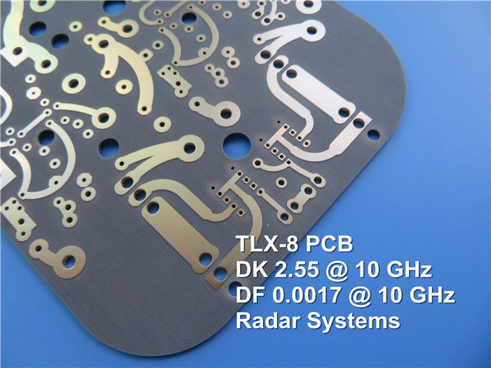
| Base Material: | Rogers, FR-4 | Layer Count: | Double Layer, Multilayer, Hybrid PCB |
|---|---|---|---|
| PCB Size: | ≤400mm X 500mm | Copper Weight: | 0.5oz (17 µm), 1oz (35µm), 2oz (70µm) |
| Surface Finish: | Bare Copper, HASL, ENIG, OSP, Immersion Tin Etc.. | ||
| High Light: | 35um High Frequency PCB,400mmx500mm High Frequency PCB,35um Radio Frequency PCB |
||
What is High Frequency PCB?
Just as its name implies, high frequency is that the frequency is relatively high, generally refers to the frequency of >=300 MHz (i.e. wave length <=1m), that is, the usual radio frequency band. The electromagnetic wave of frequency >=1GHz is called microwave.
Typical frequencies for wireless applications:
* Current mobile: 0.9GHz - 2GHz
* 3G systems: 2.5GHz
* Bluetooth: 2.5GHz
* GPS: 12.6GHz
* LMDS: 24GHz and 40GHz
* Automotive: 77GHz
Market: RFID, Wireless communications, base station and antenna, amplifier, military products, consumer electronics.
![]()
High frequency printed circuit board or microwave PCB refers to the printed circuit board made on the high frequency (microwave) substrate copper clad plate. The common types are: Double-sided board, multilayer board and mixed structure.
Mixed structure includes high performance special substrate, PP sheet + ordinary performance board and PP sheet mixed pressing board; high frequency substrate + ordinary FR4 substrate; high frequency substrate + metal base etc.
Dielectric constant
All the material in the world has a dielectric constant, it differs only in the value of the dielectric constant. The dielectric constant, also known as the capacitivity, characterizes a physical quantity of the electric polarization properties of the dielectric under the action of external electric field. The dielectric layer of PCB board is composed of different dielectric constant materials, therefore, the dielectric constant of the dielectric layer is different due to the different compositions and structures.
The PCB dielectric layer used for high frequency and high-speed digitized signal transmission is not only playing the role of insulation layer between conductors, but also plays a role of "characteristic impedance", it also affects the transmission speed of signal, signal attenuation and heating, etc.
For example, the use of 1080 glass fabric PCB, 1080 glass fabric accounted for 38% of the volume (resin accounted for 62%), its dielectric constant ER1 is 6.6 (dielectric constant of resin ER2 is 3.8), then the dielectric constant ER1080 of this PCB is: ER1080= (6.6 X 38)% + (3.8 X 62)% = 4.864.
The formula of the transmission speed of signal in a high frequency circuit:
![]()
V: The transmission speed of signal (unit is m/s)
K: constant
C: The speed of light in vacuum (unit is m/s)
Dk:dielectric constant of the substrate
Obviously, it is beneficial to improve the transmission speed of signal by reducing Dk.
It can be seen that the lower the dielectric constant of the substrate is, the faster the transmission speed of signal, therefore, to obtain a high signal transmission rate, the low and uniform dielectric constant substrate materials must be researched and developed.
![]()
Dielectric loss
When insulating material under the action of electric filed, due to the hysteresis effect of dielectric conductivity and dielectric polarization, its interior will cause energy loss which is also called dielectric loss.
The dielectric loss in the transmission loss on conductor circuit is mainly controlled by the dielectric constant (ER) and dielectric loss factor (Df) of the insulating layer of the substrate material. The effect on transmission loss is in direct proportion to the size of Er, Df, and is related to the frequency of dielectric work. Under the same Er or Df, the higher the frequency, the greater the transmission loss. With the increase of frequency, the loss in the substrate cannot be ignored, and the propagation loss or attenuation of the signal can be expressed as: A =f x Df x Er
A: signal propagation attenuation (unit: dB/m)
f: Frequency
Df: the dielectric loss factor of the substrate
Er: the dielectric constant of substrate
It can be seen that the smaller the Df of the substrate, the smaller the attenuation of signal propagation. Therefore, it is required to have a lower Er and Df when selecting the material of high frequency circuit board. In addition, there are other external factors, such as thermal performance, water absorption, etc.
![]()
The selection of high frequency material in PCB design:
The designer is suggested to consider the following key factors when selecting the board material in PCB design:
(1)FR4 can be chosen for the PCB works under 1GHz, the cost is low, and the multi-layer pressboard technology is mature.
(2)The improved epoxy resin can be selected for optical fiber communication products work over 622 Mb/s and the one work over 1G below 3GHz, because its dielectric constant is relatively stable and with low cost, the multilayer pressboard technology is the same as FR4.
(3)For large signal microwave circuits below 3GHz, such as power amplifiers and low noise amplifiers, are recommended to choose the board similar to RO4350B, the dielectric constant of RO4350B is fairly stable, with low loss factor and good heat resistance, and the processing technology is equivalent to FR4. You can see all kinds of high frequency boards that we sell in globalsources.com for reference.
![]()
(4)For microwave circuits more than 10GHz, such as power amplifiers, low noise amplifier, DUC/DDC, which have a higher requirements for boards, are recommended to use the boards with similar properties to PTFE, or the low-cost, high-performance laminates pressed with FR4 and high frequency board. You can also see the multiple mixed pressure high frequency board that we sell in globalsources.com for reference.
![]()
Processing characteristics:
1) The requirement of substrate is strict: the specified dielectric constant, dielectric thickness and copper foil thickness have been selected according to the actual impedance needs in the design of PCB, therefore, when accepting orders, it must be checked carefully, and meet the design requirements.
2)The structure of high frequency board: generally to save the cost, the composite structure of RF+FR4 are mostly used for commercial high-frequency board, warpage must be prevented in the production process.
3) The requirement of manufacture accuracy of transmission line is high: the transmission of high frequency signal is very strict for the characteristic impedance of printed wire, that is to say, the manufacturing requirement of transmission line is generally ± 1mil, and the edge of transmission line must be very neat. High frequency electrical pulse signals are transmitted in high frequency printed circuit boards instead of current. The pits, copper nodule and pinholes will affect the transmission, the higher the frequency, the greater the impact. Any burr, gap, line replenishment, open and short circuit repair, etc are not allowed.
4)The uniformity requirement of the coating layer: the characteristic impedance of the transmission line of the high frequency microwave board directly affects the transmission quality of the microwave signal. And the size of the characteristic impedance has a certain relationship with the thickness of the copper foil, especially for the hole metallized microwave board, the thickness of the coating will not only affect the total thickness of the copper foil, but also affect the accuracy of the conductor after etching, therefore, the thickness and uniformity of the coating must be strictly controlled.
5)Requirements of machining: first, the material of high-frequency microwave board is quite different from that of PCB in the processing of epoxy glass cloth; secondly, the processing accuracy of high frequency microwave board is much higher than that of FR4 PCB board, and the general form tolerance is ± 0.1mm.
6)The requirement of impedance is strict: if the content of the characteristic impedance and the most basic requirement of the high frequency microwave board, cannot meet the requirement of the characteristic impedance, then everything is useless. Dk is related to the signal transmission speed and the characteristic impedance of the PCB design, normally, the larger the impedance, the faster the signal transmission. Simply, the greater the impedance, that is, the greater the ability to prevent signals from infiltrating into the dielectric layer, the faster the signal is transmitted.
7)The line width of the signal is strictly controlled: the control requirement of characteristic impedance of the high frequency signal transmission is very strict, and the tolerance of the line width control cannot be controlled by ±20%. As the binding force of circuit is different, the etching parameters shall be adjusted or the process compensation for circuit line width shall be adjusted in time in high frequency substrate etching.
![]()
Contact Person: Ms. Ivy Deng
Tel: 86-755-27374946
Fax: 86-755-27374848